|
|
|
PDF 74LVC374A Data sheet ( Hoja de datos )
| Número de pieza | 74LVC374A | |
| Descripción | OCTAL D-TYPE FLIP-FLOP | |
| Fabricantes | STMicroelectronics | |
| Logotipo | ||
Hay una vista previa y un enlace de descarga de 74LVC374A (archivo pdf) en la parte inferior de esta página. Total 14 Páginas | ||
|
No Preview Available !
74LVC374A
OCTAL D-TYPE FLIP-FLOP
HIGH PERFORMANCE
s 5V TOLERANT INPUTS
s HIGH SPEED: tPD = 6.8ns (MAX.) at VCC = 3V
s POWER DOWN PROTECTION ON INPUTS
AND OUTPUTS
s SYMMETRICAL OUTPUT IMPEDANCE:
)|IOH| = IOL = 24mA (MIN) at VCC = 3V
t(ss PCI BUS LEVELS GUARANTEED AT 24 mA
SOP
TSSOP
cs BALANCED PROPAGATION DELAYS:
utPLH ≅ tPHL
ds OPERATING VOLTAGE RANGE:
roVCC(OPR) = 1.65V to 3.6V (1.2V Data
PRetention)
tes PIN AND FUNCTION COMPATIBLE WITH
74 SERIES 374
Table 1: Order Codes
PACKAGE
SOP
TSSOP
T&R
74LVC374AMTR
74LVC374ATTR
les LATCH-UP PERFORMANCE EXCEEDS
o500mA (JESD 17)
bss ESD PERFORMANCE:
OHBM > 2000V (MIL STD 883 method 3015);
-MM > 200V
t(s)DESCRIPTION
The 74LVC374A is an advanced high-speed
ucCMOS OCTAL D-TYPE FLIP FLOP with 3 STATE
dOUTPUTS NON INVERTING fabricated with
rosub-micron silicon gate and double-layer metal
wiring C2MOS technology.
PThese 8 bit D-Type latch are controlled by a clock
teinput (CK) and an output enable input (OE).
leOn the positive transition of the clock, the Q
ooutputs will be set to the logic state that were
ssetup at the D inputs.
While the (OE) input is low, the 8 outputs will be in
a normal logic state (high or low logic level) and
while high level the outputs will be in a high
impedance state.
The Output control does not affect the internal
operation of flip flops; that is, the old data can be
retained or the new data can be entered even
while the outputs are off. Power down protection is
provided on all inputs and 0 to 7V can be accepted
on inputs with no regard to the supply voltage.
This device can be used to interface 5V to 3V.
All inputs and outputs are equipped with
protection circuits against static discharge, giving
them 2KV ESD immunity and transient excess
voltage.
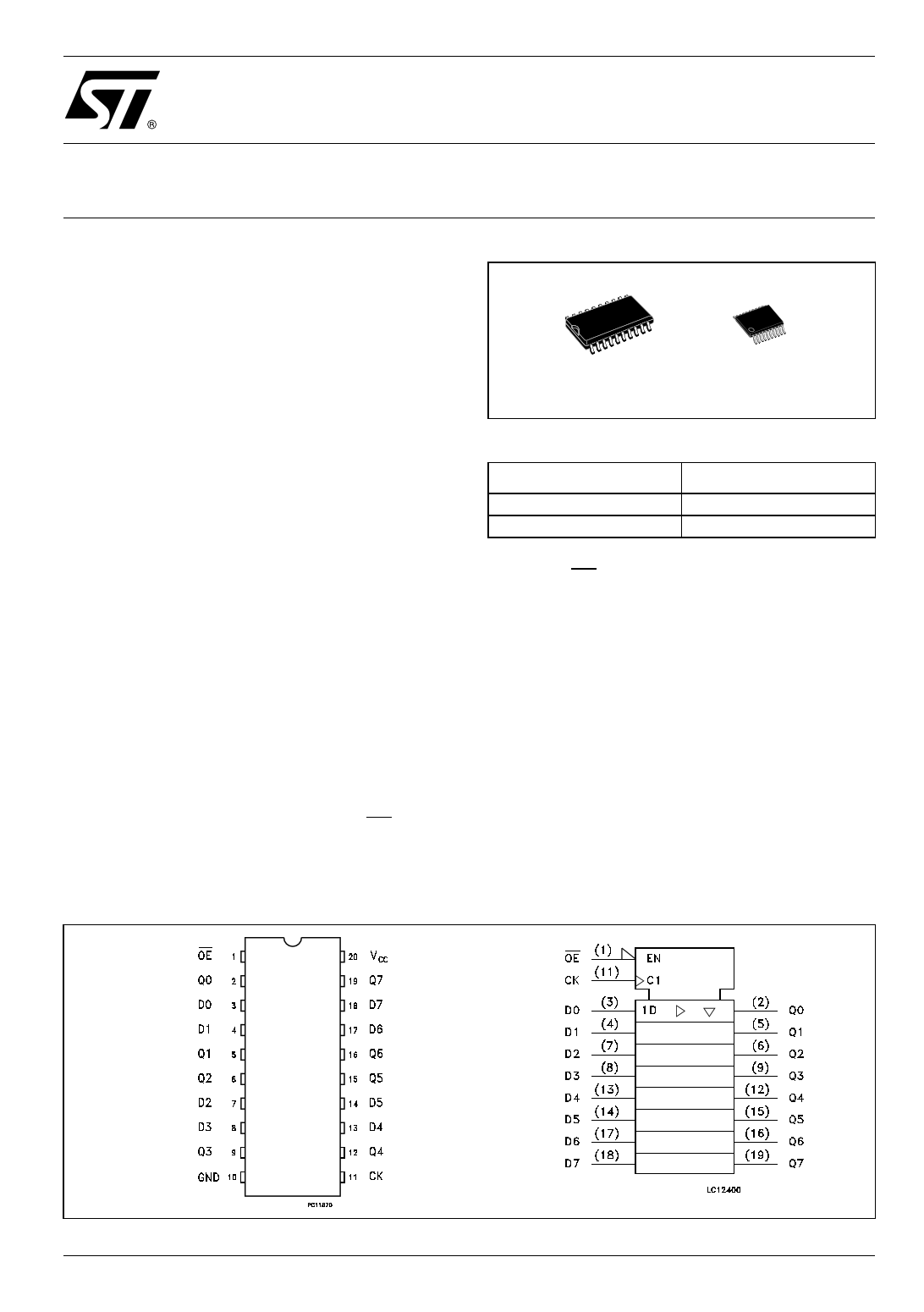
ObFigure 1: Pin Connection And IEC Logic Symbols
July 2004
Rev. 2
1/14
1 page 
74LVC374A
Table 8: AC Electrical Characteristics
Test Condition
Value
Symbol
Parameter
VCC
CL RL ts = tr -40 to 85 °C
-55 to 125 °C Unit
(V) (pF) (Ω) (ns) Min. Max. Min. Max.
tPLH tPHL Propagation Delay 1.65 to 1.95 30 1000 2.0
TBD
TBD
Time D to Q
2.3 to 2.7 30 500 2.0
TBD
TBD
ns
2.7 50 500 2.5 1.5 7.8 1.5 9.4
3.0 to 3.6 50 500 2.5
1
6.8
1
8.2
tPLH tPHL Propagation Delay 1.65 to 1.95 30 1000 2.0
TBD
TBD
Time LE to Q
2.3 to 2.7 30 500 2.0
2.7 50 500 2.5
t(s)3.0 to 3.6 50 500 2.5
tPZL tPZH Output Enable Time 1.65 to 1.95 30 1000 2.0
c2.3 to 2.7 30 500 2.0
du2.7 50 500 2.5
ro3.0 to 3.6 50 500 2.5
PtPLZ tPHZ Output Disable Time 1.65 to 1.95 30 1000 2.0
2.3 to 2.7 30 500 2.0
te2.7 50 500 2.5
le3.0 to 3.6 50 500 2.5
sotW LE Pulse Width
bHIGH
1.65 to 1.95 30 1000 2.0
2.3 to 2.7 30 500 2.0
O2.7 50 500 2.5
-3.0 to 3.6 50 500 2.5
)ts Setup Time D to LE 1.65 to 1.95 30 1000 2.0
t(s(HIGH to LOW)
2.3 to 2.7 30 500 2.0
c2.7 50 500 2.5
u3.0 to 3.6 50 500 2.5
dth Hold Time D to
1.65 to 1.95 30 1000 2.0
roCLOCK, HIGH or
2.3 to 2.7 30 500 2.0
PLOW
2.7 50 500 2.5
te 3.0 to 3.6 50 500 2.5
letOSLH
sotOSHL
Output To Output
Skew Time (note1,
2)
2.7 to 3.6
1.5
1
1
1
2
2
TBD
TBD
3.3
3.3
TBD
TBD
2
2
TBD
TBD
1.5
1.5
TBD
7.8
6.8
TBD
TBD
8.7
7.7
TBD
TBD
7.6
7.0
1
1.5
1
1
1
2
2
TBD
TBD
3.3
3.3
TDB
TBD
2
2
TBD
TBD
1.5
1.5
TBD
9.4
8.2
TBD
TBD
10.4
9.2
TBD
TBD
9.1
8.4
1
ns
ns
ns
ns
ns
ns
ns
b1) Skew is defined as the absolute value of the difference between the actual propagation delay for any two outputs of the same device switch-
Oing in the same direction, either HIGH or LOW (tOSLH = | tPLHm - tPLHn|, tOSHL = | tPHLm - tPHLn|
2) Parameter guaranteed by design
Table 9: Capacitive Characteristics
Test Condition
Value
Symbol
Parameter
CIN Input Capacitance
CPD Power Dissipation Capacitance
(note 1)
VCC
(V)
1.8
2.5
3.3
fIN = 10MHz
TA = 25 °C
Min. Typ. Max.
4
28
30
34
Unit
pF
pF
1) CPD is defined as the value of the IC’s internal equivalent capacitance which is calculated from the operating current consumption without
load. (Refer to Test Circuit). Average operating current can be obtained by the following equation. ICC(opr) = CPD x VCC x fIN + ICC/n (per circuit)
5/14
5 Page 
74LVC374A
Tape & Reel SO-20 MECHANICAL DATA
DIM.
MIN.
mm.
TYP
MAX.
MIN.
inch
TYP.
MAX.
A 330 12.992
C 12.8
13.2 0.504
0.519
D 20.2
0.795
N 60
t(s)T
cAo 10.8
duBo 13.2
roKo 3.1
PPo 3.9
Obsolete Product(s) - ObsoleteP 11.9
2.362
30.4
11 0.425
13.4 0.520
3.3 0.122
4.1 0.153
12.1 0.468
1.197
0.433
0.528
0.130
0.161
0.476
11/14
11 Page | ||
| Páginas | Total 14 Páginas | |
| PDF Descargar | [ Datasheet 74LVC374A.PDF ] | |
Hoja de datos destacado
| Número de pieza | Descripción | Fabricantes |
| 74LVC374A | Octal D-type flip-flop | NXP Semiconductors |
| 74LVC374A | Octal D-type flip-flop | Philips |
| 74LVC374A | OCTAL D-TYPE FLIP-FLOP | STMicroelectronics |
| 74LVC374A | OCTAL D-TYPE FLIP-FLOP | Diodes |
| Número de pieza | Descripción | Fabricantes |
| SLA6805M | High Voltage 3 phase Motor Driver IC. |
Sanken |
| SDC1742 | 12- and 14-Bit Hybrid Synchro / Resolver-to-Digital Converters. |
Analog Devices |
|
DataSheet.es es una pagina web que funciona como un repositorio de manuales o hoja de datos de muchos de los productos más populares, |
| DataSheet.es | 2020 | Privacy Policy | Contacto | Buscar |