|
|
PDF NCV70514 Data sheet ( Hoja de datos )
| Número de pieza | NCV70514 | |
| Descripción | Micro-stepping Motor Driver | |
| Fabricantes | ON Semiconductor | |
| Logotipo | ||
Hay una vista previa y un enlace de descarga de NCV70514 (archivo pdf) en la parte inferior de esta página. Total 30 Páginas | ||
|
No Preview Available !
NCV70514
Micro-stepping Motor Driver
Description
The NCV70514 is a micro−stepping stepper motor driver for bipolar
stepper motors. The chip is connected through I/O pins and an SPI
interface with an external microcontroller. The NCV70514 contains
a current−translation table and takes the next micro−step depending on
the clock signal on the “NXT” input pin and the status of the “DIR”
(= direction) register or input pin. The chip provides an error message
if stall, an electrical error, an under−voltage or an elevated junction
temperature is detected. It is using a proprietary PWM algorithm
for reliable current control.
NCV70514 is fully compatible with the automotive voltage
requirements and is ideally suited for general−purpose stepper motor
applications in the automotive, industrial, medical, and marine
environment.
Due to the technology, the device is especially suited for use
in applications with fluctuating battery supplies.
www.onsemi.com
1 32
QFN32, 5x5
CASE 488AM
MARKING
DIAGRAM
1
N70514−x
AWLYYWW
G
Features
• Dual H−bridge for 2−phase Stepper Motors
• Programmable Peak−current up to 800 mA
• Low Temperature Boost Current
(available only for NCV70514MW007 device)
• On−chip Current Translator
• SPI Interface with Daisy Chain Capability
• 7 Step Modes from Full−step up to 32 Micro−steps
• Fully Integrated Current−sensing and Current−regulation
• On Chip Stall Detection
• PWM Current Control with Automatic Selection of Fast and Slow
Decay
• Fixed PWM Frequency
• Active Fly−back Diodes
• Full Output Protection and Diagnosis
• Thermal Warning and Shutdown
• Compatible with 3.3 V Microcontrollers, 5 V Tolerant Inputs, 5 V
N70514 = Specific Device Code
A = Assembly Location
WL = Wafer Lot
YY = Year
WW = Work Week
G = Pb−Free Package
ORDERING INFORMATION
See detailed ordering and shipping information in the package
dimensions section on page 30 of this data sheet.
Tolerant Open Drain Outputs
• Reset Function
• Overcurrent Protection
• Enhanced Under Voltage Management
• Step Mode Selection Inputs
• These Devices are Pb−Free, Halogen Free/BFR Free and are RoHS Compliant
Typical Applications
• Small Positioning Applications
• Automotive (headlamp alignment, HVAC, idle control, cruise control)
• Industrial Equipment (lighting, fluid control, labeling, process control, XYZ tables, robots)
• Building Automation (HVAC, surveillance, satellite dish, renewable energy systems)
© Semiconductor Components Industries, LLC, 2016
October, 2016 − Rev. 3
1
Publication Order Number:
NCV70514/D
1 page 
NCV70514
Table 3. ABSOLUTE MAXIMUM RATINGS
Characteristic
Symbol
Min Max Unit
Supply voltage (Note 6)
VBB −0.3 +40 V
Digital input/outputs voltage
VIO −0.3 +6.0 V
Junction temperature range (Note 7)
Tj
−45
+175
°C
Storage Temperature (Note 8)
Tstrg
−55
+160
°C
HBM Electrostatic discharge voltage (Note 9)
Vesd_hbm
−2 +2 kV
System Electrostatic discharge voltage (Note 10)
Vsyst_esd
−8 +8 kV
Stresses exceeding those listed in the Maximum Ratings table may damage the device. If any of these limits are exceeded, device functionality
should not be assumed, damage may occur and reliability may be affected.
6. VBB Max is +43 V for limited time <0.5 s.
7. The circuit functionality is not guaranteed.
8. For limited time up to 100 hours. Otherwise the max storage temperature is 85°C.
9. HBM according to AEC−Q100: EIA−JESD22−A114−B (100 pF via 1.5 kW).
10. System ESD, 150 pF, 330 W, contact discharge on the connector pin, unpowered.
Operating ranges define the limits for functional
operation and parametric characteristics of the device. A
mission profile (Note 11) is a substantial part of the
operation conditions; hence the Customer must contact
ON Semiconductor in order to mutually agree in writing on
the allowed missions profile(s) in the application.
Table 4. RECOMMENDED OPERATING RANGES
Characteristic
Symbol
Min Typ Max Unit
Battery Supply voltage
VBB +6
+29 V
Digital input/outputs voltage
VIO 0
+5.5
V
Parametric operating junction temperature range (Notes 12, 14)
Tjp
−40
+145
°C
Functional operating junction temperature range (Notes 13, 14) Tjf −40
+160
°C
Functional operation above the stresses listed in the Recommended Operating Ranges is not implied. Extended exposure to stresses beyond
the Recommended Operating Ranges limits may affect device reliability.
11. A mission profile describes the application specific conditions such as, but not limited to, the cumulative operating conditions over life time,
the system power dissipation, the system’s environmental conditions, the thermal design of the customer’s system, the modes, in which the
device is operated by the customer, etc. No more than 100 cumulated hours in life time above Ttw.
12. The parametric characteristics of the circuit are not guaranteed outside the Parametric operating junction temperature range.
13. The maximum functional operating temperature range can be limited by thermal shutdown Ttsd.
14. The cold boost motor current shall be enabled only for ambient temperature below 25°C.
PACKAGE THERMAL CHARACTERISTIC
The NCV70514 is available in thermally optimized
QFN32 5x5 package. For the optimizations, the package has
an exposed thermal pad which has to be soldered to the PCB
ground plane. The ground plane needs thermal vias to
conduct the heat to the bottom layer.
For precise thermal cooling calculations the major
thermal resistances of the devices are given. The thermal
media to which the power of the devices has to be given are:
• Static environmental air (via the case)
• PCB board copper area (via the device pins and
exposed pad)
The major thermal resistances of the device are the Rth
from the junction to the ambient (Rthja) and the Rth from the
junction to the exposed pad (Rthjp).
Using an exposed die pad on the bottom surface of the
package is mainly contributing to this performance. In order
to take full advantage of the exposed pad, it is most
important that the PCB has features to conduct heat away
from the package. In the table below, one can find the values
for the Rthja and Rthjp:
Table 5. THERMAL RESISTANCE
Package
Rth, Junction−to−Exposed Pad, Rthjp
Rth, Junction−to−Ambient, Rthja (Note 15)
QFN32 5x5
15 K/W
39 K/W
15. The Rthja for 2S2P simulated for worst case power and following conditions:
• A 4−layer printed circuit board with inner power planes and outer (top and bottom) signal layers is used
• Board thickness is 1.46 mm (FR4 PCB material)
• All four layers: 30 um thick copper with an area of 2500 mm2 where:
− Top layer with 70% copper coverage in 20x20 mm around device, rest 40% copper coverage
− In layer 1 with 70% copper coverage
− In layer 2 with 98% copper coverage
− Bottom layer with 90% copper coverage
• The 12 vias in Exposed Pad area, via diameter 0.4 mm
• Gap−filler max 400 mm between PCB and heat sink non conductive with worst case thermal conductivity of 1.5 W/mK
www.onsemi.com
5
5 Page 
NCV70514
DETAILED OPERATING DESCRIPTION
H−Bridge Drivers with PWM Control
Two H−bridges are integrated to drive a bipolar stepper
motor. Each H−bridge consists of two low−side N−type
MOSFET switches and two high−side P−type MOSFET
switches. One PWM current control loop with on−chip
current sensing is implemented for each H−bridge.
Depending on the desired current range and the micro−step
position at hand, the RDS(on) of the low−side transistors will
be adapted to maintain current−sense accuracy. A
comparator compares continuously the actual winding
current with the requested current and feeds back the
information to generate a PWM signal, which turns on/off
the H−bridge switches. The switching points of the PWM
duty−cycle are synchronized to the on−chip PWM clock. For
each output bridge the PWM duty cycle is measured and
stored in two appropriate status registers of the motor
controller.
The PWM frequency will not vary with changes in the
supply voltage. Also variations in motor−speed or load−
conditions of the motor have no effect. There are no external
components required to adjust the PWM frequency. In order
to avoid large currents through the H−bridge switches, it is
guaranteed that the top− and bottom−switches of the same
half−bridge are never conductive simultaneously (interlock
delay).
In order to reduce the radiated/conducted emission,
voltage slope control is implemented in the output switches.
Two bits in SPI control register 3 allow adjustment of the
voltage slopes.
A protection against shorts on motor lines is implemented.
When excessive voltage is sensed across a MOSFET for a
time longer than the required transition time, then the
MOSFET is switched−off.
Motor Enable−Disable
The H−bridges and PWM control can be disabled
(high−impedance state) by means of a bit <MOTEN> in the
SPI control registers. <MOTEN>=0 will only disable the
drivers and will not impact the functions of NXT, DIR,
RHB, SPI bus, etc. The H−bridges will resume normal PWM
operation by writing <MOTEN>=1 in the SPI register.
PWM current control is then enabled again and will regulate
current in both coils corresponding with the position given
by the current translator.
Automatic Forward and Slow−Fast Decay
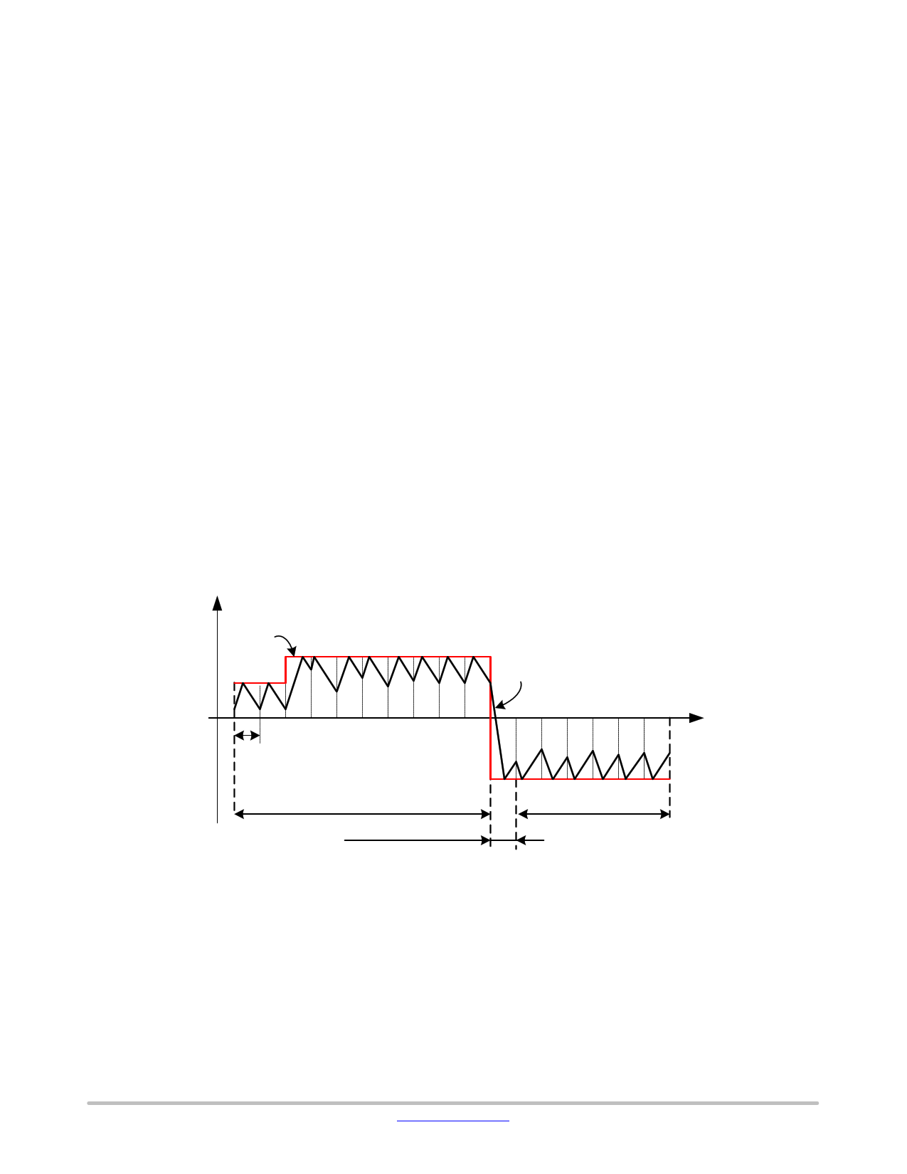
The PWM generation is in steady−state using a
combination of forward and slow−decay. For transition to
lower current levels, fast−decay is automatically activated to
allow high−speed response. The selection of fast or slow
decay is completely transparent for the user and no
additional parameters are required for operation.
Icoil
Set value
0
tpwm
Actual value
t
Forward & Slow Decay
Fast Decay & Forward
Forward & Slow Decay
Figure 7. Forward and Slow/Fast Decay PWM
www.onsemi.com
11
11 Page | ||
| Páginas | Total 30 Páginas | |
| PDF Descargar | [ Datasheet NCV70514.PDF ] | |
Hoja de datos destacado
| Número de pieza | Descripción | Fabricantes |
| NCV70514 | Micro-stepping Motor Driver | ON Semiconductor |
| Número de pieza | Descripción | Fabricantes |
| SLA6805M | High Voltage 3 phase Motor Driver IC. |
Sanken |
| SDC1742 | 12- and 14-Bit Hybrid Synchro / Resolver-to-Digital Converters. |
Analog Devices |
|
DataSheet.es es una pagina web que funciona como un repositorio de manuales o hoja de datos de muchos de los productos más populares, |
| DataSheet.es | 2020 | Privacy Policy | Contacto | Buscar |
