|
|
|
PDF M25PE80 Data sheet ( Hoja de datos )
| Número de pieza | M25PE80 | |
| Descripción | page-erasable serial flash memory | |
| Fabricantes | Numonyx | |
| Logotipo | ||
Hay una vista previa y un enlace de descarga de M25PE80 (archivo pdf) en la parte inferior de esta página. Total 30 Páginas | ||
|
No Preview Available !
M25PE80
8-Mbit, page-erasable serial flash memory with
byte alterability, 75 MHz SPI bus, standard pinout
Features
■ SPI bus compatible serial interface
■ 8-Mbit page-erasable flash memory
■ Page size: 256 bytes
– Page write in 11 ms (typical)
– Page program in 0.8 ms (typical)
– Page erase in 10 ms (typical)
■ Subsector erase (4 Kbytes)
■ Sector erase (64 Kbytes)
■ Bulk erase (8 Mbits)
■ 2.7 V to 3.6 V single supply voltage
■ 75 MHz clock rate (maximum)
■ Deep power-down mode 1 µA (typical)
■ Electronic signature
– JEDEC standard two-byte signature
(8014h)
– Unique ID code (UID) with 16 bytes read-
only, available upon customer request only
in the T9HX process
■ Software write protection on a 64-Kbyte sector
basis
■ Hardware write protection of the memory area
selected using the BP0, BP1 and BP2 bits
■ More than 100 000 write cycles
■ More than 20 years data retention
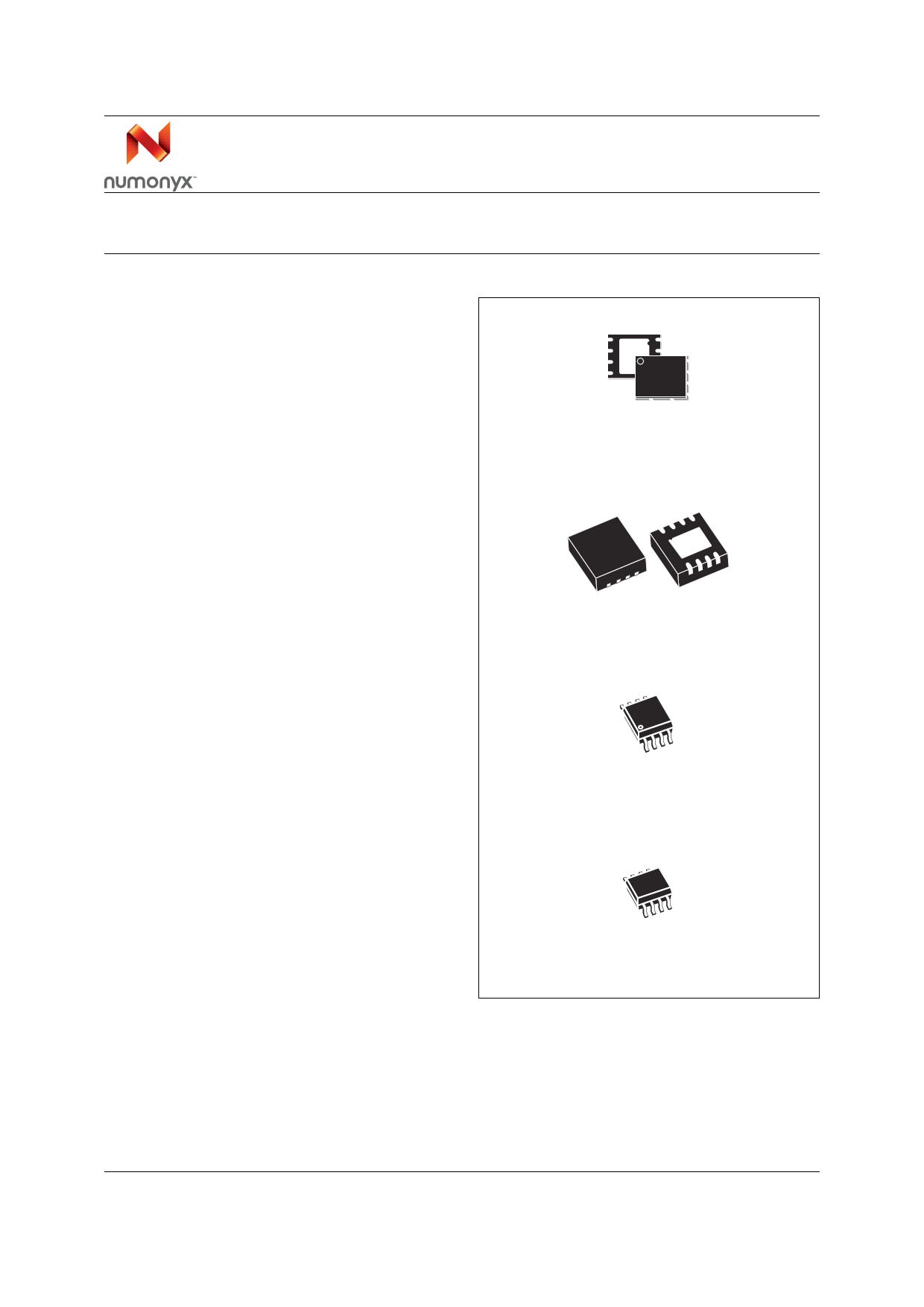
■ Packages
– ECOPACK® (RoHS compliant)
VFQFPN8 (MP)
6 x 5 mm (MLP8)
QFN8L (MS)
6 x 5 mm (MLP8)
SO8W (MW)
208 mils width
SO8N (MN)
150 mils width
April 2008
Rev 7
1/66
www.numonyx.com
1
1 page 
M25PE80
List of figures
List of figures
Figure 1.
Figure 2.
Figure 3.
Figure 4.
Figure 5.
Figure 6.
Figure 7.
Figure 8.
Figure 9.
Figure 10.
Figure 11.
Figure 12.
Figure 13.
Figure 14.
Figure 15.
Figure 16.
Figure 17.
Figure 18.
Figure 19.
Figure 20.
Figure 21.
Figure 22.
Figure 23.
Figure 24.
Figure 25.
Figure 26.
Figure 27.
Figure 28.
Figure 29.
Figure 30.
Figure 31.
Figure 32.
Figure 33.
Logic diagram - previous T7Y process . . . . . . . . . . . . . . . . . . . . . . . . . . . . . . . . . . . . . . . . . 7
Logic diagram - new T9HX process . . . . . . . . . . . . . . . . . . . . . . . . . . . . . . . . . . . . . . . . . . . 7
VFQFPN, QFN8L and SO connections . . . . . . . . . . . . . . . . . . . . . . . . . . . . . . . . . . . . . . . . 7
Bus master and memory devices on the SPI bus . . . . . . . . . . . . . . . . . . . . . . . . . . . . . . . . 10
SPI modes supported . . . . . . . . . . . . . . . . . . . . . . . . . . . . . . . . . . . . . . . . . . . . . . . . . . . . . 11
Block diagram . . . . . . . . . . . . . . . . . . . . . . . . . . . . . . . . . . . . . . . . . . . . . . . . . . . . . . . . . . . 19
Write enable (WREN) instruction sequence . . . . . . . . . . . . . . . . . . . . . . . . . . . . . . . . . . . . 22
Write disable (WRDI) instruction sequence . . . . . . . . . . . . . . . . . . . . . . . . . . . . . . . . . . . . 22
Read Identification (RDID) instruction sequence and data-out sequence . . . . . . . . . . . . . 24
Read status register (RDSR) instruction sequence and data-out sequence . . . . . . . . . . . 26
Write status register (WRSR) instruction sequence . . . . . . . . . . . . . . . . . . . . . . . . . . . . . . 27
Read data bytes (READ) instruction sequence and data-out sequence . . . . . . . . . . . . . . 29
Read data bytes at higher speed (FAST_READ) instruction sequence
and data-out sequence . . . . . . . . . . . . . . . . . . . . . . . . . . . . . . . . . . . . . . . . . . . . . . . . . . . . 30
Read lock register (RDLR) instruction sequence and data-out sequence . . . . . . . . . . . . . 32
Page write (PW) instruction sequence . . . . . . . . . . . . . . . . . . . . . . . . . . . . . . . . . . . . . . . . 34
Page program (PP) instruction sequence . . . . . . . . . . . . . . . . . . . . . . . . . . . . . . . . . . . . . . 36
Write to lock register (WRLR) instruction sequence . . . . . . . . . . . . . . . . . . . . . . . . . . . . . . 37
Page erase (PE) instruction sequence . . . . . . . . . . . . . . . . . . . . . . . . . . . . . . . . . . . . . . . . 40
Subsector erase (SSE) instruction sequence . . . . . . . . . . . . . . . . . . . . . . . . . . . . . . . . . . . 41
Sector erase (SE) instruction sequence . . . . . . . . . . . . . . . . . . . . . . . . . . . . . . . . . . . . . . . 42
Bulk erase (BE) instruction sequence. . . . . . . . . . . . . . . . . . . . . . . . . . . . . . . . . . . . . . . . . 43
Deep power-down (DP) instruction sequence . . . . . . . . . . . . . . . . . . . . . . . . . . . . . . . . . . 44
Release from deep power-down (RDP) instruction sequence . . . . . . . . . . . . . . . . . . . . . . 45
Power-up timing . . . . . . . . . . . . . . . . . . . . . . . . . . . . . . . . . . . . . . . . . . . . . . . . . . . . . . . . . 47
AC measurement I/O waveform . . . . . . . . . . . . . . . . . . . . . . . . . . . . . . . . . . . . . . . . . . . . . 50
Serial input timing . . . . . . . . . . . . . . . . . . . . . . . . . . . . . . . . . . . . . . . . . . . . . . . . . . . . . . . . 55
Top sector lock (T7Y process) or write protect (T9HX process) setup and hold
timing . . . . . . . . . . . . . . . . . . . . . . . . . . . . . . . . . . . . . . . . . . . . . . . . . . . . . . . . . . . . . . . . . 55
Output timing . . . . . . . . . . . . . . . . . . . . . . . . . . . . . . . . . . . . . . . . . . . . . . . . . . . . . . . . . . . 56
Reset AC waveforms . . . . . . . . . . . . . . . . . . . . . . . . . . . . . . . . . . . . . . . . . . . . . . . . . . . . . 57
VFQFPN8 (MLP8) 8-lead very thin dual flat package no lead, 6 × 5 mm,
package outline. . . . . . . . . . . . . . . . . . . . . . . . . . . . . . . . . . . . . . . . . . . . . . . . . . . . . . . . . . 58
QFN8L (MLP8) 8-lead, quad flat package no lead, 6 × 5 mm, package outline . . . . . . . . . 60
SO8 wide – 8 lead plastic small outline, 208 mils body width, package outline . . . . . . . . . 61
SO8N - 8 lead plastic small outline, 150 mils body width, package outline . . . . . . . . . . . . 62
5/66
5 Page 
M25PE80
SPI modes
Example: Cp = 50 pF, that is R*Cp = 5 µs <=> the application must ensure that the Bus
Master never leaves the SPI bus in the high impedance state for a time period shorter than
5 µs.
Figure 5. SPI modes supported
CPOL CPHA
0 0C
1 1C
D MSB
Q MSB
AI01438B
11/66
11 Page | ||
| Páginas | Total 30 Páginas | |
| PDF Descargar | [ Datasheet M25PE80.PDF ] | |
Hoja de datos destacado
| Número de pieza | Descripción | Fabricantes |
| M25PE80 | 8Mb 3V NOR Serial Flash Memory | Micron |
| M25PE80 | page-erasable serial flash memory | Numonyx |
| M25PE80 | Page-Erasable Serial Flash memory | ST Microelectronics |
| Número de pieza | Descripción | Fabricantes |
| SLA6805M | High Voltage 3 phase Motor Driver IC. |
Sanken |
| SDC1742 | 12- and 14-Bit Hybrid Synchro / Resolver-to-Digital Converters. |
Analog Devices |
|
DataSheet.es es una pagina web que funciona como un repositorio de manuales o hoja de datos de muchos de los productos más populares, |
| DataSheet.es | 2020 | Privacy Policy | Contacto | Buscar |