|
|
|
PDF ADuM4190 Data sheet ( Hoja de datos )
| Número de pieza | ADuM4190 | |
| Descripción | High Stability Isolated Error Amplifier | |
| Fabricantes | Analog Devices | |
| Logotipo | ||
Hay una vista previa y un enlace de descarga de ADuM4190 (archivo pdf) en la parte inferior de esta página. Total 21 Páginas | ||
|
No Preview Available !
Data Sheet
High Stability Isolated Error Amplifier
ADuM4190
FEATURES
Stable over time and temperature
0.5% initial accuracy
1% accuracy over the full temperature range
Compatible with Type II or Type III compensation networks
Reference voltage: 1.225 V
Compatible with DOSA
Low power operation: <7 mA total
Wide voltage supply range
VDD1: 3 V to 20 V
VDD2: 3 V to 20 V
Bandwidth: 400 kHz
Isolation voltage: 5 kV rms reinforced
Safety and regulatory approvals (pending)
UL recognition: 5000 V rms for 1 minute per UL 1577
CSA Component Acceptance Notice #5A
VDE certificate of conformity
DIN V VDE V 0884-10 (VDE V 0884-10):2006-12
VIORM = 849 V peak
Wide temperature range
−40°C to +125°C ambient operation
150°C maximum junction temperature
APPLICATIONS
Linear feedback power supplies
Inverters
Uninterruptible power supplies (UPS)
DOSA-compatible modules
Voltage monitors
GENERAL DESCRIPTION
The ADuM41901 is an isolated error amplifier based on Analog
Devices, Inc., iCoupler® technology. The ADuM4190 is ideal for
linear feedback power supplies. The primary side controllers of
the ADuM4190 enable improvements in transient response, power
density, and stability as compared to commonly used optocoupler
and shunt regulator solutions.
Unlike optocoupler-based solutions, which have an uncertain
current transfer ratio over lifetime and at high temperatures, the
ADuM4190 transfer function does not change over its lifetime
and is stable over a wide temperature range of −40°C to +125°C.
Included in the ADuM4190 is a wideband operational amplifier
for a variety of commonly used power supply loop compensation
techniques. The ADuM4190 is fast enough to allow a feedback loop
to react to fast transient conditions and overcurrent conditions.
Also included is a high accuracy 1.225 V reference to compare
with the supply output setpoint.
The ADuM4190 is packaged in a wide body, 16-lead SOIC package
for a reinforced 5 kV rms isolation voltage rating.
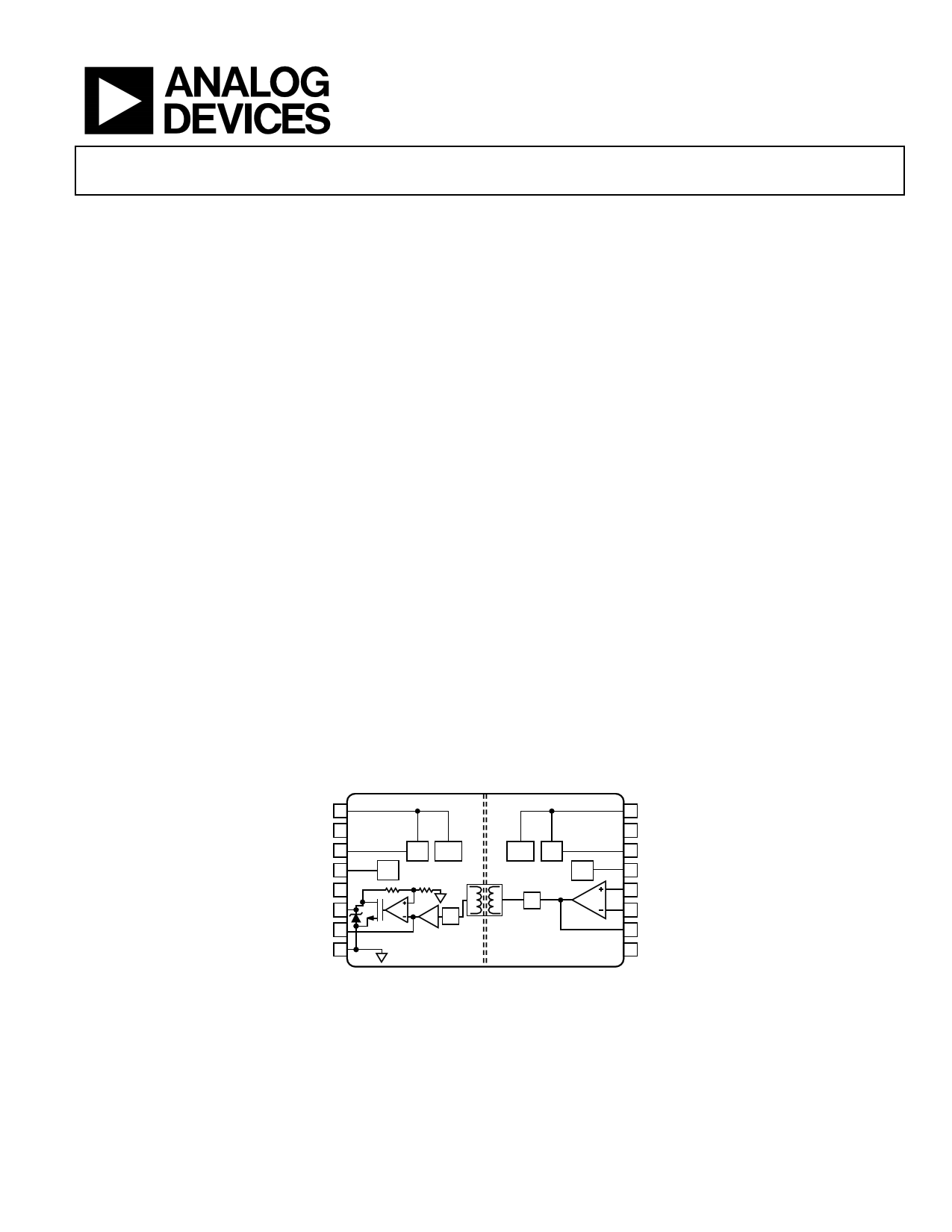
FUNCTIONAL BLOCK DIAGRAM
VDD1 1
GND1 2
VREG1 3
REFOUT1 4
NC 5
EAOUT2 6
EAOUT 7
GND1 8
REG UVLO
REF
Rx
UVLO REG
REF
Tx
Figure 1.
ADuM4190
16 VDD2
15 GND2
14 VREG2
13 REFOUT
12 +IN
11 –IN
10 COMP
9 GND2
1 Protected by U.S. Patents 5,952,849; 6,873,065; and 7,075,329. Other patents pending.
Rev. 0
Document Feedback
Information furnished by Analog Devices is believed to be accurate and reliable. However, no
responsibilityisassumedbyAnalogDevices for itsuse,nor foranyinfringementsofpatentsor other
rights of third parties that may result from its use. Specifications subject to change without notice. No
license is granted by implication or otherwise under any patent or patent rights of Analog Devices.
Trademarksandregisteredtrademarksarethepropertyoftheirrespectiveowners.
One Technology Way, P.O. Box 9106, Norwood, MA 02062-9106, U.S.A.
Tel: 781.329.4700
©2013 Analog Devices, Inc. All rights reserved.
Technical Support
www.analog.com
1 page 
ADuM4190
Data Sheet
Parameter
Power Supply Rejection
Supply Current
IDD1
IDD2
Test Conditions/Comments
DC, VDD1 = VDD2 = 3 V to 20 V
See Figure 4
See Figure 5
Min Typ Max Unit
60 dB
1.4 2.0 mA
2.9 5.0 mA
1 Output gain is defined as the slope of the best-fit line of the output voltage vs. the input voltage over the specified input range, with the offset error adjusted out.
2 Output linearity is defined as the peak-to-peak output deviation from the best-fit line of the output gain, expressed as a percentage of the full-scale output voltage.
PACKAGE CHARACTERISTICS
Table 2.
Parameter
RESISTANCE
Input-to-Output1
CAPACITANCE
Input-to-Output1
Input Capacitance2
IC JUNCTION-TO-AMBIENT THERMAL
RESISTANCE
Symbol Min
RI-O
CI-O
CI
θJA
Typ Max
1013
2.2
4.0
45
Unit Test Conditions/Comments
Ω
pF
pF
°C/W
f = 1 MHz
Thermocouple located at center of package
underside
1 The device is considered a 2-terminal device; Pin 1 through Pin 8 are shorted together, and Pin 9 through Pin 16 are shorted together.
2 Input capacitance is from any input pin to ground.
REGULATORY INFORMATION
The ADuM4190 is pending approval by the organizations listed in Table 3. See Table 8 and the Insulation Lifetime section for recommended
maximum working voltages for specific cross-isolation waveforms and insulation levels.
Table 3.
UL (Pending)
Recognized under UL 1577 component
recognition program1
Single protection, 5000 V rms isolation
voltage, 16-lead SOIC
File E214100
CSA (Pending)
Approved under CSA Component Acceptance
Notice #5A
Reinforced insulation per CSA 60950-1-03 and
IEC 60950-1, 400 V rms (565 V peak) maximum
working voltage
Basic insulation per CSA 60950-1-03 and IEC
60950-1, 800 V rms (1131 V peak) maximum
working voltage
File 205078
VDE (Pending)
Certified according to DIN V VDE V 0884-10
(VDE V 0884-10):2006-122
Reinforced insulation, 849 V peak
File 2471900-4880-0001
1 In accordance with UL 1577, each ADuM4190 is proof tested by applying an insulation test voltage ≥ 6000 V rms for 1 sec (current leakage detection limit = 10 µA).
2 In accordance with DIN V VDE V 0884-10 (VDE V 0884-10):2006-12, each ADuM4190 is proof tested by applying an insulation test voltage ≥ 1590 V peak for 1 sec
(partial discharge detection limit = 5 pC). The asterisk (*) marking branded on the component designates DIN V VDE V 0884-10 (VDE V 0884-10):2006-12 approval.
INSULATION AND SAFETY RELATED SPECIFICATIONS
Table 4.
Parameter
Rated Dielectric Insulation Voltage
Minimum External Air Gap (Clearance)
Symbol
L(I01)
Value
5000
8.0 min
Unit
V rms
mm
Minimum External Tracking (Creepage)
Minimum Internal Gap (Internal Clearance)
Tracking Resistance (Comparative Tracking Index)
Isolation Group
L(I02)
CTI
8.3 min mm
0.017 min
>400
II
mm
V
Test Conditions/Comments
1-minute duration
Measured from input terminals to output
terminals, shortest distance through air
along the PCB mounting plane, as an aid
to PCB layout
Measured from input terminals to output
terminals, shortest distance path along body
Insulation distance through insulation
DIN IEC 112/VDE 0303, Part 1
Material Group DIN VDE 0110, 1/89, Table 1
Rev. 0 | Page 4 of 20
5 Page 
ADuM4190
30
25
20
15
10
5
0
0.90 0.95 1.00 1.05
COMP TO EAOUT GAIN (V/V)
Figure 16. EAOUT Gain Distribution at 25°C
1.10
30
25
20
15
10
5
0
0.90 0.95 1.00 1.05
COMP TO EAOUT GAIN (V/V)
Figure 17. EAOUT Gain Distribution at 125°C
1.10
30
25
20
15
10
5
0
0.90 0.95 1.00 1.05
COMP TO EAOUT GAIN (V/V)
Figure 18. EAOUT Gain Distribution at −40°C
1.10
Data Sheet
30
25
20
15
10
5
0
–0.4 –0.2
0
0.2 0.4
COMP TO EAOUT OFFSET VOLTAGE (V)
Figure 19. EAOUT Offset Voltage Distribution at 25°C
30
25
20
15
10
5
0
–0.4
–0.2
0
0.2 0.4
COMP TO EAOUT OFFSET VOLTAGE (V)
Figure 20. EAOUT Offset Voltage Distribution at 125°C
30
25
20
15
10
5
0
–0.4 –0.2
0
0.2 0.4
COMP TO EAOUT OFFSET VOLTAGE (V)
Figure 21. EAOUT Offset Voltage Distribution at −40°C
Rev. 0 | Page 10 of 20
11 Page | ||
| Páginas | Total 21 Páginas | |
| PDF Descargar | [ Datasheet ADuM4190.PDF ] | |
Hoja de datos destacado
| Número de pieza | Descripción | Fabricantes |
| ADuM4190 | High Stability Isolated Error Amplifier | Analog Devices |
| Número de pieza | Descripción | Fabricantes |
| SLA6805M | High Voltage 3 phase Motor Driver IC. |
Sanken |
| SDC1742 | 12- and 14-Bit Hybrid Synchro / Resolver-to-Digital Converters. |
Analog Devices |
|
DataSheet.es es una pagina web que funciona como un repositorio de manuales o hoja de datos de muchos de los productos más populares, |
| DataSheet.es | 2020 | Privacy Policy | Contacto | Buscar |