|
|
PDF TGA2216-SM Data sheet ( Hoja de datos )
| Número de pieza | TGA2216-SM | |
| Descripción | 10W GaN Power Amplifier | |
| Fabricantes | TriQuint Semiconductor | |
| Logotipo | ||
Hay una vista previa y un enlace de descarga de TGA2216-SM (archivo pdf) en la parte inferior de esta página. Total 18 Páginas | ||
|
No Preview Available !
Applications
Commercial and military radar
Communications
Electronic Warfare
TGA2216-SM
0.1 – 3.0GHz 10W GaN Power Amplifier
Product Features
Frequency Range: 0.1 – 3.0GHz
PSAT: >40dBm at PIN = 27dBm
P1dB: >35dBm
PAE: 50% @ midband
Large Signal Gain: >13dB
Small Signal Gain: 21dB
Bias: VD = 40V, IDQ = 360mA, VG1 = -2.4V Typical,
VG2 = +17.7V Typical
Wideband Flat Gain and Power
Package Dimensions: 5.0 x 5.0 x 1.45 mm
QFN 5x5 mm 32L
Functional Block Diagram
32 31 30 29 28 27 26 25
1
2
3
4
RF IN 5
6
7
8
24
23
22
21
20 RF OUT
19
18
17
9 10 11 12 13 14 15 16
General Description
Pad Configuration
TriQuint’s TGA2216-SM is a wideband cascode amplifier
fabricated on TriQuint’s production 0.25um GaN on SiC
process. The cascode configuration offers exceptional
wideband performance as well as supporting 40V
operation. The TGA2216-SM operates from 0.1 - 3.0GHz
and provides greater than 10W of saturated output power
with greater than 13dB of large signal gain and greater
than 40% power-added efficiency.
The TGA2216-SM is available in a low-cost, surface
mount 32 lead 5x5 AIN QFN. It is ideally suited to
support both radar and communication applications
across defense and commercial markets as well as
electronic warfare. The TGA2216-SM is fully matched to
50Ω at both RF ports allowing for simple system
integration. DC blocks are required on both RF ports and
the drain voltage must be injected through an off chip
bias-tee on the RF output port.
Lead-free and RoHS compliant.
Evaluation boards are available upon request.
Pad No.
Symbol
1-2, 4, 6, 8-9, 16-17, 19, 21, 23-25, 32 GND
3, 7, 10-11, 13, 15, 18, 22, 26, 28, 30-31 NC
5 RF IN
12, 29
GATE1
14, 27
20
GATE 2
RF OUT,
DRAIN
Ordering Information
Part
TGA2216-SM
ECCN
EAR99
Description
0.1 – 3.0GHz 10W
GaN Power Amplifier
Preliminary Datasheet: Rev - 05-05-14
© 2014 TriQuint
- 1 of 18 -
Disclaimer: Subject to change without notice
www.triquint.com
1 page 
TGA2216-SM
0.1 – 3.0GHz 10W GaN Power Amplifier
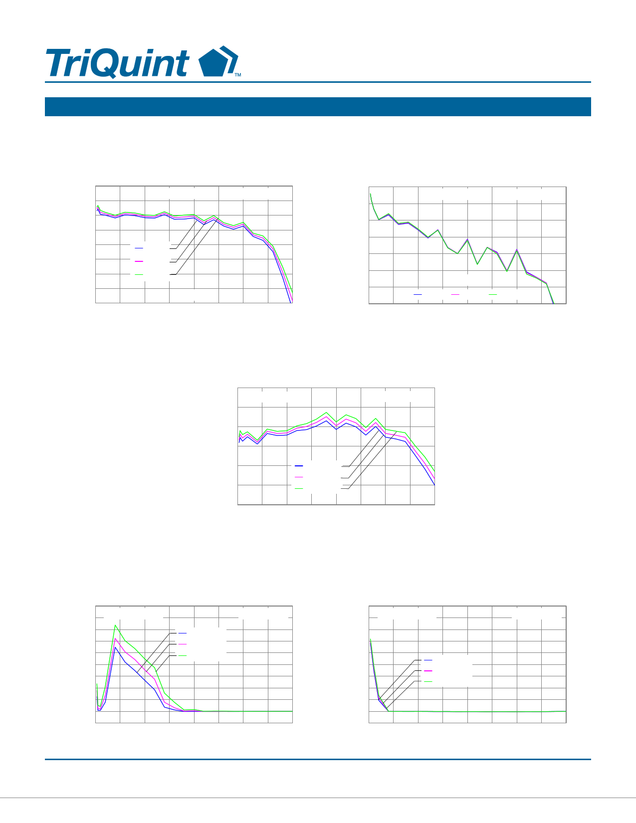
Typical Performance: Large Signal (CW)
The plots reflect performance measured with an external coaxial bias tee and DC blocks
(See application circuit on page 11)
Output Power vs. Frequency vs. IDQ
43
42
Temp. = +25°C
PIN = 27dBm
41
40
39 120mA
38 240mA
37 360mA
36
VD = 40V
35
0 0.5 1 1.5 2 2.5 3 3.5 4
Frequency (GHz)
65
60
55
50
45
40
35
30
0
PAE vs. Frequency vs. IDQ
Temp. = +25°C
PIN = 27dBm
VD = 40V
120mA 240mA
360mA
0.5 1 1.5 2 2.5 3 3.5 4
Frequency (GHz)
800 Drain Current vs. Frequency vs. IDQ
Temp. = +25°C
PIN = 27dBm
700
600
500
400 40V120mA
40V240mA
300 40V360mA
200
0 0.5 1 1.5 2 2.5 3 3.5 4
Frequency (GHz)
4.5 Gate1 Current vs. Frequency vs. IDQ
4.0 Temp. = +25°C
PIN = 27dBm
3.5 40V120mA
3.0 40V240mA
2.5 40V360mA
2.0
1.5
1.0
0.5
0.0
-0.5
0 0.5 1 1.5 2 2.5 3 3.5 4
Frequency (GHz)
4.5 Gate2 Current vs. Frequency vs. IDQ
4.0 Temp. = +25°C
PIN = 27dBm
3.5
3.0
2.5
2.0 40V120mA
40V240mA
1.5
40V360mA
1.0
0.5
0.0
-0.5
0 0.5 1 1.5 2 2.5 3 3.5 4
Frequency (GHz)
Preliminary Datasheet: Rev - 05-05-14
© 2014 TriQuint
- 5 of 18 -
Disclaimer: Subject to change without notice
www.triquint.com
5 Page 
TGA2216-SM
0.1 – 3.0GHz 10W GaN Power Amplifier
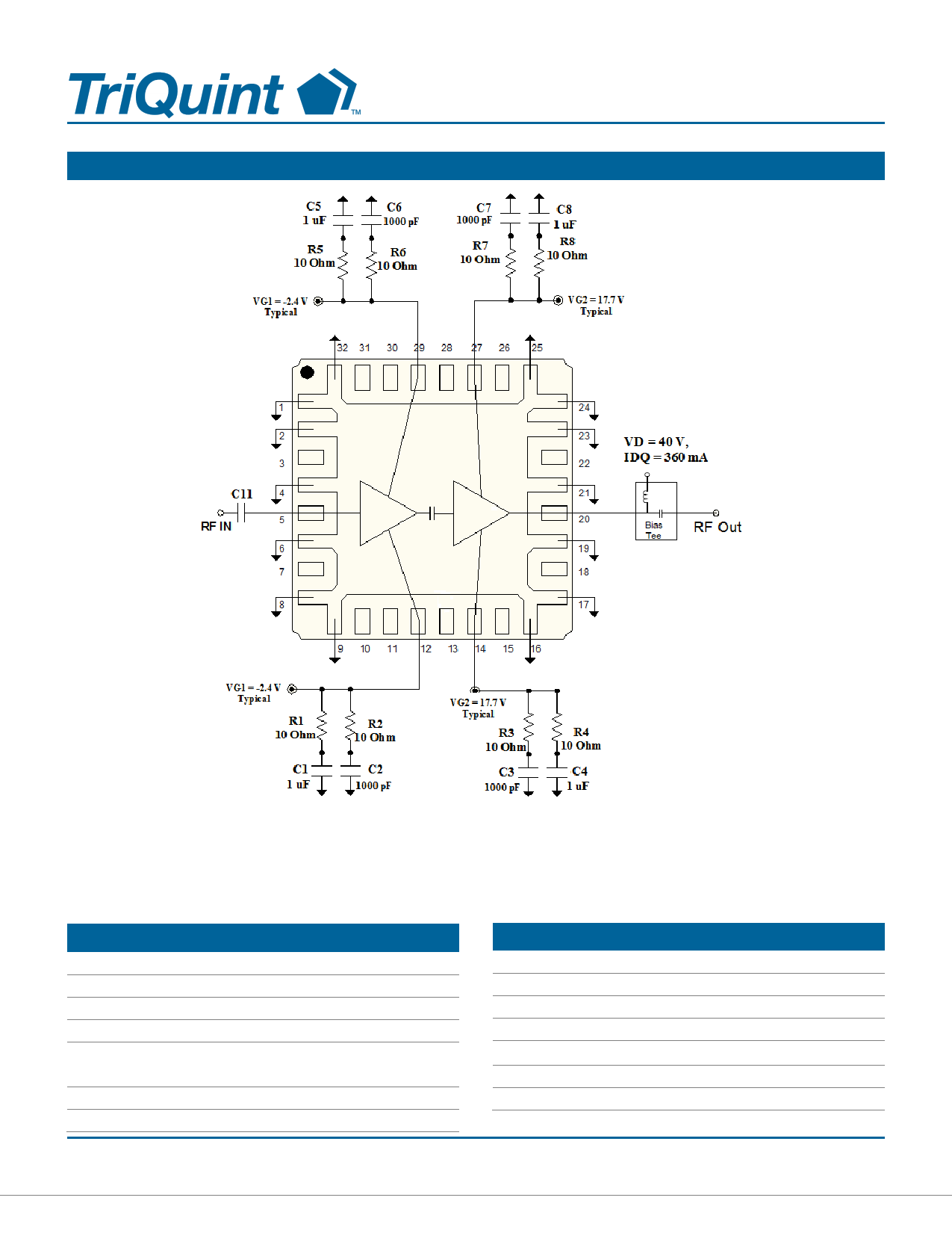
Application Circuit (Coaxial input DC block and coaxial output bias tee)
Notes:
1.
2.
3.
VG1 & VG2 can be biased from either side (Top or Bottom.)
Coaxial input DC block (C11) is used for input port (RF In.)
External wide bandwidth Bias-Tee is used for output port (RF Out). VD is applied through the output Bias-
Tee.
Bias-up Procedure
Bias-down Procedure
1. Set ID limit to 720mA, IG1 & IG2 limit to 5mA
2. Set VG1 to -5.0V
3. Set VG2 to (VD/2) - 2.7V or 40V/2 - 2.7V = 17.3V
4. Set VD +40V
1. Turn off RF signal
2. Reduce VG1 to -5.0V. Ensure IDQ ~ 0mA
3. Reduce VG2 to 0V.
4. Set VD to 0V
5. Adjust VG1 more positive until IDQ = 360mA (VG1 ~ -
2.4V Typical)
6. Adjust VG2 to (VD/2) + VG1; (VG2 ~ +17.7V Typical)
7. Apply RF signal
5. Turn off VD supply
6. Turn off VG2 supply
7. Turn off VG1 supply
Preliminary Datasheet: Rev - 05-05-14
© 2014 TriQuint
- 11 of 18 -
Disclaimer: Subject to change without notice
www.triquint.com
11 Page | ||
| Páginas | Total 18 Páginas | |
| PDF Descargar | [ Datasheet TGA2216-SM.PDF ] | |
Hoja de datos destacado
| Número de pieza | Descripción | Fabricantes |
| TGA2216-SM | 10W GaN Power Amplifier | TriQuint Semiconductor |
| Número de pieza | Descripción | Fabricantes |
| SLA6805M | High Voltage 3 phase Motor Driver IC. |
Sanken |
| SDC1742 | 12- and 14-Bit Hybrid Synchro / Resolver-to-Digital Converters. |
Analog Devices |
|
DataSheet.es es una pagina web que funciona como un repositorio de manuales o hoja de datos de muchos de los productos más populares, |
| DataSheet.es | 2020 | Privacy Policy | Contacto | Buscar |
