|
|
PDF GT24C512 Data sheet ( Hoja de datos )
| Número de pieza | GT24C512 | |
| Descripción | 2-WIRE 512K Bits Serial EEPROM | |
| Fabricantes | Giantec Semiconductor | |
| Logotipo | ||
Hay una vista previa y un enlace de descarga de GT24C512 (archivo pdf) en la parte inferior de esta página. Total 20 Páginas | ||
|
No Preview Available !
GT24C512
GT24C512
2-WIRE
512K Bits
Serial EEPROM
Copyright © 2013 Giantec Semiconductor Inc. (Giantec). All rights reserved. Giantec reserves the right to make changes to this specification and its products at any time without
notice. Giantec products are not designed, intended, authorized or warranted for use as components in systems or equipment intended for critical medical or surgical equipment,
aerospace or military, or other applications planned to support or sustain life. It is the customer's obligation to optimize the design in their own products for the best performance
and optimization on the functionality and etc. Giantec assumes no liability arising out of the application or use of any information, products or services described herein. Customers
are advised to obtain the latest version of this device specification before relying on any published information and prior placing orders for products.
Giantec Semiconductor, Inc.
vo
www.giantec-semi.com
1/20
1 page 
GT24C512
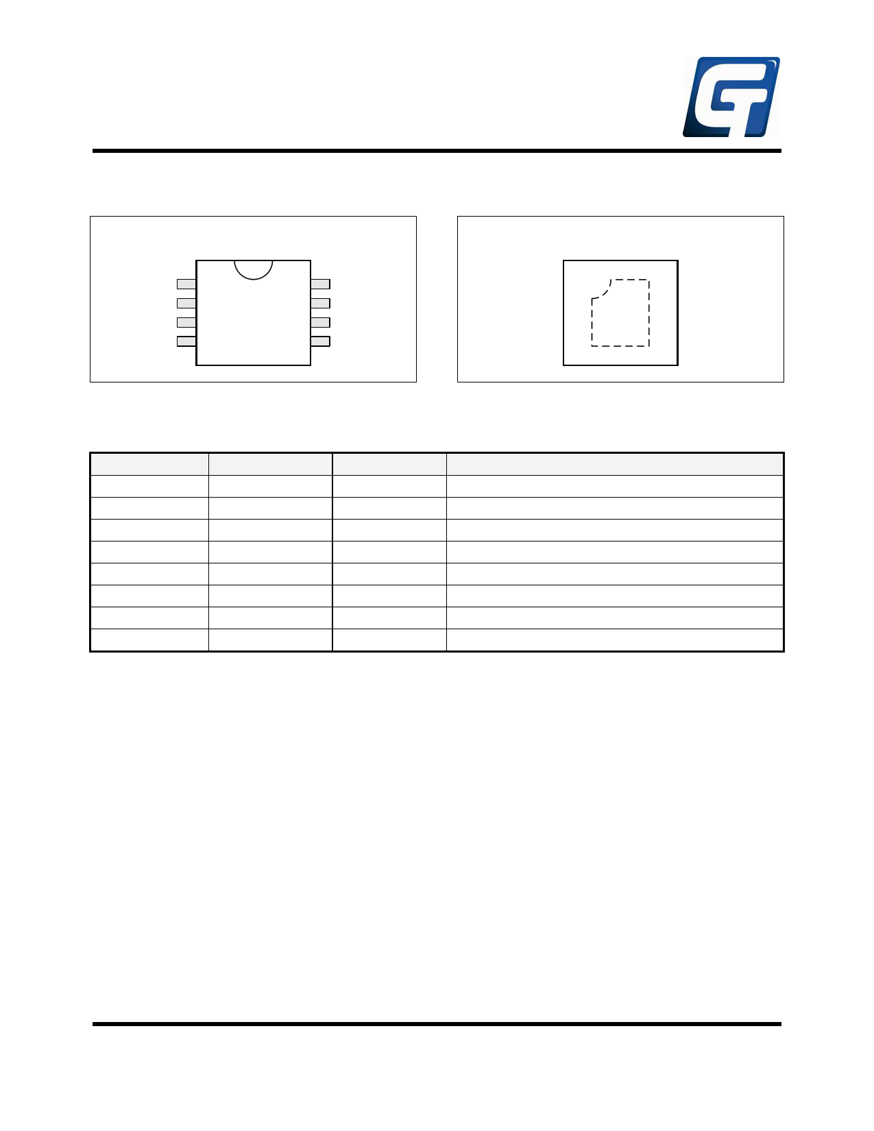
4. Pin Configuration
4.1 8-Pin SOIC/SOP and TSSOP
Top View
A0
A1
A2
GND
1
2
3
4
8 VCC
7 WP
6 SCL
5 SDA
4.2 8-Lead DFN
Top View
A0 1
A1 2
A2 3
GND 4
8 VCC
7 WP
6 SCL
5 SDA
4.3 Pin Definition
Pin No.
1
2
3
4
5
6
7
8
Pin Name
A0
A1
A2
GND
SDA
SCL
WP
VCC
I/O Definition
I Device Address Input
I Device Address Input
I Device Address Input
- Ground
I/O Serial Address and Data input and Data out put
I Serial Clock Input
I Write Protect Input
- Power Supply
4.4 Pin Descriptions
SCL
This input clock pin is used to synchronize the data transfer
to and from the device.
SDA
The SDA is a bi-directional pin used to transfer addresses
and data into and out of the device. The SDA pin is an open
drain output and can be wired with other open drain or open
collector outputs. However, the SDA pin requires a pull-up
resistor connected to the power supply.
A0, A1, A2
The A0, A1 and A2 are the device address inputs.
Typically, the A0, A1, and A2 pins are for hardware
addressing and a total of 8 devices can be connected on a
Giantec Semiconductor, Inc.
v0
single bus system. When A0, A1, and A2 are left floating,
the inputs are defaulted to zero.
WP
WP is the Write Protect pin. While the WP pin is connected
to the power supply of GT24C512, the entire array becomes
Write Protected (i.e. the device becomes Read only). When
WP is tied to Ground or left floating, the normal write
operations are allowed.
VCC
Supply voltage
GND
Ground of supply voltage
www.giantec-semi.com
5/20
5 Page 
GT24C512
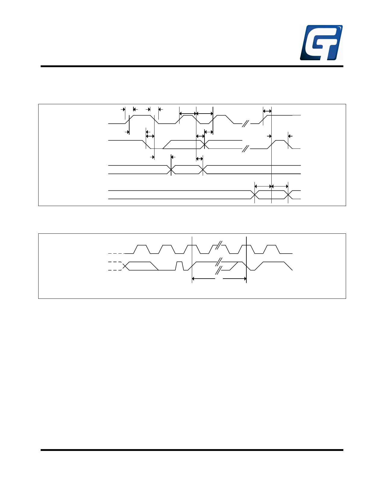
5.12 Timing Diagrams
SCL
SDAIN
SDAOUT
Figure 5-11. Bus Timing
TR TF
THIGH TLOW
TSU:STA
THD:STA
THD:DAT
TSU:DAT
TAA TDH
WP
TSU:STO
TBUF
TSU:WP THD:WP
Figure 5-12. Write Cycle Timing
SCL
SDA
Word n
ACK
TWR
STOP
Condition
START
Condition
Giantec Semiconductor, Inc.
v0
www.giantec-semi.com
11/20
11 Page | ||
| Páginas | Total 20 Páginas | |
| PDF Descargar | [ Datasheet GT24C512.PDF ] | |
Hoja de datos destacado
| Número de pieza | Descripción | Fabricantes |
| GT24C512 | 2-WIRE 512K Bits Serial EEPROM | Giantec Semiconductor |
| Número de pieza | Descripción | Fabricantes |
| SLA6805M | High Voltage 3 phase Motor Driver IC. |
Sanken |
| SDC1742 | 12- and 14-Bit Hybrid Synchro / Resolver-to-Digital Converters. |
Analog Devices |
|
DataSheet.es es una pagina web que funciona como un repositorio de manuales o hoja de datos de muchos de los productos más populares, |
| DataSheet.es | 2020 | Privacy Policy | Contacto | Buscar |
