|
|
|
PDF NJG1812ME4 Data sheet ( Hoja de datos )
| Número de pieza | NJG1812ME4 | |
| Descripción | HIGH POWER DPDT SWITCH GaAs MMIC | |
| Fabricantes | New Japan Radio | |
| Logotipo | ||
Hay una vista previa y un enlace de descarga de NJG1812ME4 (archivo pdf) en la parte inferior de esta página. Total 13 Páginas | ||
|
No Preview Available !
NJG1812ME4
HIGH POWER DPDT SWITCH GaAs MMIC
GENERAL DESCRIPTION
The NJG1812ME4 is a GaAs DPDT switch MMIC suitable for
antenna swapping of LTE/UMTS/CDMA/GSM applications.
The NJG1812ME4 features very low insertion loss, low distortion
and excellent linearity performance down to 1.8V 1bit control voltage
at high frequency up to 3GHz. In addition, this switch is able to
handle high power signals.
The NJG1812ME4 has ESD protection devices to achieve
excellent ESD performances. No DC Blocking capacitors are
required for all RF ports unless DC is biased externally. And the
small & thin EQFN12-E4 package is adopted.
PACKAGE OUTLINE
NJG1812ME4
APPLICATIONS
Antenna swapping, General purpose switching applications
LTE, UMTS, CDMA, GSM systems
FEATURES
Low voltage logic control
VCTL(H)=1.35V to 5.0V
Low voltage operation
VDD=2.7V typ.
Low insertion loss
0.25dB typ. @f=900MHz, PIN=+35dBm
0.35dB typ. @f=1900MHz, PIN=+33dBm
0.45dB typ. @f=2700MHz, PIN=+27dBm
Low distortion
2nd harmonics=-89dBm typ. @ f=786.5MHz, PIN=+23dBm
3rd harmonics=-89dBm typ. @ f=710MHz, PIN=+23dBm
P-0.1dB
+36 dBm min.
Ultra-small and ultra-thin package
EQFN12-E4 (Package size: 2.0 x 2.0 x 0.397 mm typ.)
RoHS compliant and Halogen Free, MSL1
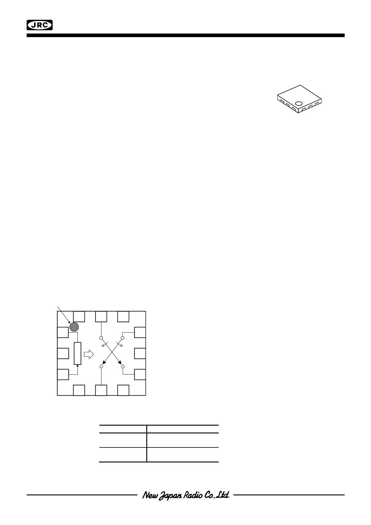
PIN CONFIGURATION
(TOP VIEW)
1PIN INDEX GND P3 GND
12 11 10
VDD 1
9 P4
GND 2
8 GND
VCTL 3
7 P1
Pin connection
1. VDD
7. P1
2. GND
8. NC(GND)
3. VCTL
9. P4
4. GND
10. NC(GND)
5. P2
11. P3
6. GND
12. GND
Exposed PAD: GND
4
GND
TRUTH TABLE
56
P2 GND
VCTL
L
H
“H”=VCTL(H), “L”=VCTL(L)
Path
P1-P4
P2-P3
P1-P3
P2-P4
Ver.2016-06 -13
-1-
1 page 
NJG1812ME4
TERMINAL INFORMATION
No.
1
2
3
4
5
6
7
8
9
10
11
12
Exposed
Pad
SYMBOL
VDD
GND
VCTL
GND
P2
GND
P1
NC(GND)
P4
NC(GND)
P3
GND
GND
DESCRIPTION
Positive voltage supply terminal. The positive voltage (+2.4 to +5V) has to be
supplied. Please connect a bypass capacitor with GND terminal for excellent
RF performance.
Ground terminal. Please connect this terminal with ground plane as close as
possible for excellent RF performance.
Control signal input terminal. This terminal is set to High-Level (+1.35 to
+5.0V) or Low-Level (0 to +0.45V).
Ground terminal. Please connect this terminal with ground plane as close as
possible for excellent RF performance.
RF transmitting/receiving port. No DC blocking capacitor is required for this
port unless DC is biased externally. Please connect an inductor with GND
terminal for ESD protection.
Ground terminal. Please connect this terminal with ground plane as close as
possible for excellent RF performance.
RF transmitting/receiving port. No DC blocking capacitor is required for this
port unless DC is biased externally. Please connect an inductor with GND
terminal for ESD protection.
No connected terminal. Please connect this terminal with ground plane as
close as possible for excellent RF performance.
RF transmitting/receiving port. No DC blocking capacitor is required for this
port unless DC is biased externally.
No connected terminal. Please connect this terminal with ground plane as
close as possible for excellent RF performance.
RF transmitting/receiving port. No DC blocking capacitor is required for this
port unless DC is biased externally.
Ground terminal. Please connect this terminal with ground plane as close as
possible for excellent RF performance.
Ground terminal. Please connect this terminal with ground plane as close as
possible for excellent RF performance.
-5-
5 Page 
EVALUATION BOARD
(Top View)
1Pin INDEX
NJG1812ME4
P2 P3 PCB (FR-4):
t=0.2mm
MICROSTRIP LINE WIDTH=0.37mm (Z0=50)
C1 PCB SIZE=26mm x 26mm
Losses of PCB and connectors, Ta=+25°C
Frequency [GHz]
0.9
1.9
2.7
Loss [dB]
0.23
0.43
0.55
PCB LAYOUT GUIDELINE (EQFN12-E4)
32 1
4 12
5 11
6 10
78 9
PCB
PKG Terminal
PKG Outline
GND Via Hole
Diameterφ=0.3mm
GND Via Hole
Diameterφ=0.2mm
PRECAUTIONS
[1] For avoiding the degradation of RF performance, the bypass capacitor (C1) should be placed as close as
possible to VDD terminal
[2] For good RF performance, all GND terminals are must be connected to PCB ground plane of substrate, and
through - holes for GND should be placed near the IC.
[3] Please connect Exposed PAD to PCB ground plane of substrate, and through - holes for GND should be placed
under the IC.
- 11 -
11 Page | ||
| Páginas | Total 13 Páginas | |
| PDF Descargar | [ Datasheet NJG1812ME4.PDF ] | |
Hoja de datos destacado
| Número de pieza | Descripción | Fabricantes |
| NJG1812ME4 | HIGH POWER DPDT SWITCH GaAs MMIC | New Japan Radio |
| Número de pieza | Descripción | Fabricantes |
| SLA6805M | High Voltage 3 phase Motor Driver IC. |
Sanken |
| SDC1742 | 12- and 14-Bit Hybrid Synchro / Resolver-to-Digital Converters. |
Analog Devices |
|
DataSheet.es es una pagina web que funciona como un repositorio de manuales o hoja de datos de muchos de los productos más populares, |
| DataSheet.es | 2020 | Privacy Policy | Contacto | Buscar |