|
|
|
PDF ADSP-SC571 Data sheet ( Hoja de datos )
| Número de pieza | ADSP-SC571 | |
| Descripción | SHARC+ Dual Core DSP | |
| Fabricantes | Analog Devices | |
| Logotipo | ||
Hay una vista previa y un enlace de descarga de ADSP-SC571 (archivo pdf) en la parte inferior de esta página. Total 30 Páginas | ||
|
No Preview Available !
SHARC+ Dual Core
DSP with ARM Cortex-A5
Preliminary Technical Data ADSP-SC570/571/572/573/ADSP-21571/21573
SYSTEM FEATURES
Dual enhanced SHARC+ high performance floating-point
cores
Up to 450 MHz per SHARC+ core
Up to 3M bits (384 kB) L1SRAM memory per core with
parity (optional ability to configure as cache)
32-bit, 40-bit, and 64-bit floating-point support
32-bit fixed point
Byte, short-word, word, long-word addressed
ARM Cortex-A5 core
450 MHz/720 DMIPS with Neon/VFPv4-D16/Jazelle
32 kB L1 instruction cache with parity/32 kB L1 data cache
with parity
256 kB L2 cache with parity
Powerful DMA system
On-chip memory protection
Integrated safety features
17 mm × 17 mm 400-ball CSP BGA and 176-lead LQFP-EP,
RoHS compliant
Low system power across automotive temperature range
MEMORY
Large on-chip L2 SRAM with ECC protection, up to 1MB
One L3 interface optimized for low system power, providing
16-bit interface to DDR3, DDR2 or LPDDR1 SDRAM devices
ADDITIONAL FEATURES
Security and Protection
Crypto hardware accelerators
Fast secure boot with IP protection
Support for TrustZone®
Accelerators
FIR, IIR, offload engines
SYSTEM CONTROL
SECURITY AND PROTECTION
SYSTEM PROTECTION (SPU)
SYSTEM MEMORY
PROTECTION UNIT (SMPU)
FAULT MANAGEMENT
ARM® TrustZone® SECURITY
DUAL CRC
WATCHDOGS
OTP MEMORY
THERMAL MONITOR UNIT (TMU)
PROGRAM FLOW
SYS EVENT CONTROLLER (SEC)
TRIGGER ROUTING (TRU)
CLOCK, RESET, AND POWER
CLOCK GENERATION (CGU)
CLOCK DISTRIBUTION
UNIT (CDU)
RESET CONTROL (RCU)
POWER MANAGEMENT (DPM)
DEBUG UNIT
ARM® CoreSightTM
WATCHPOINTS (SWU)
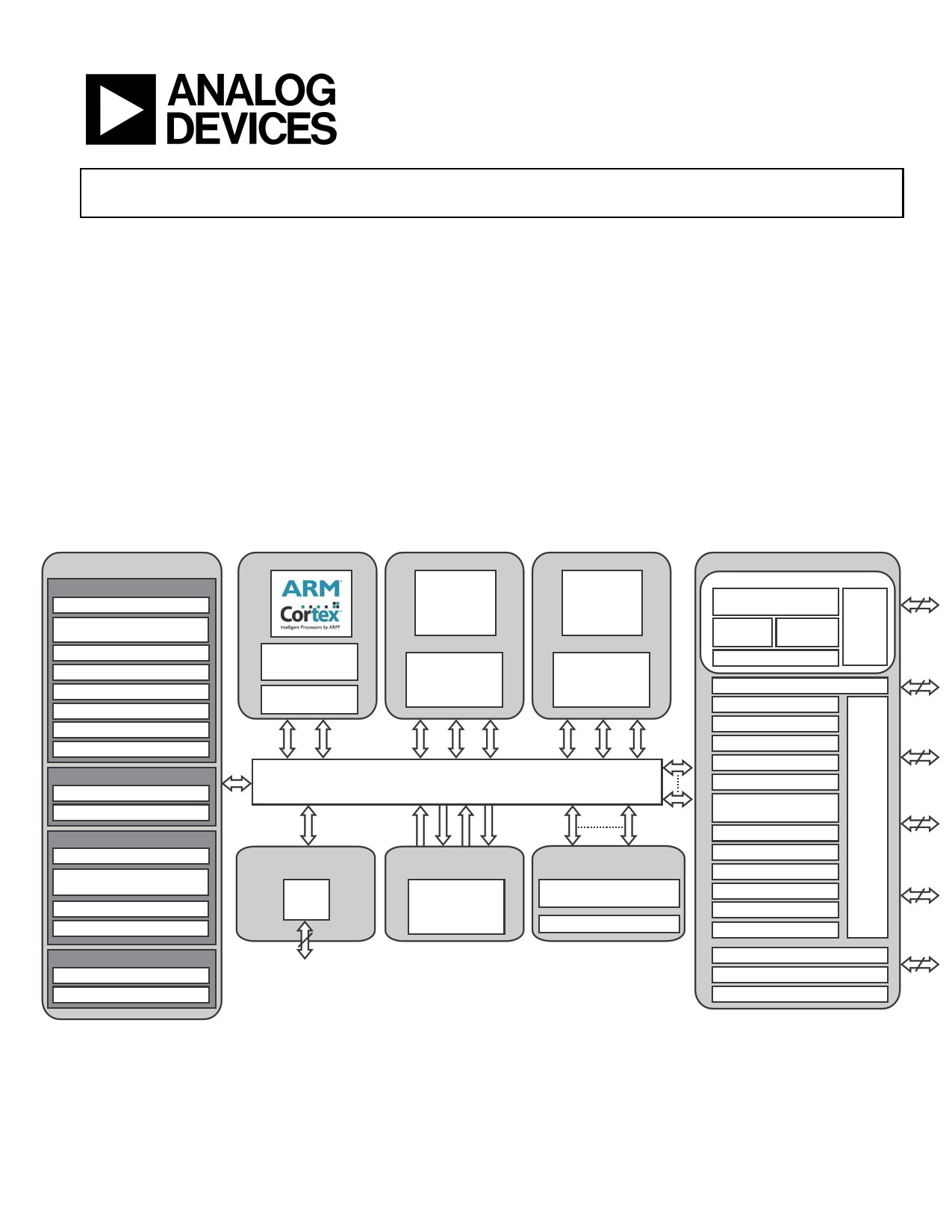
CORE 0
L1 CACHE (PARITY)
32 kB L1 I-CACHE
32 kB L1 D-CACHE
L2 CACHE
256 kB (PARITY)
CORE 1
S
L1 SRAM (PARITY)
3M BITS (384 kB)
SRAM/CACHE
CORE 2
S
L1 SRAM (PARITY)
3M BITS (384 kB)
SRAM/CACHE
SYSTEM CROSSBAR AND DMA SUBSYSTEM
L3 MEMORY
INTERFACE
DDR3
DDR2
LPDDR1
16
DATA
SYSTEM
L2 MEMORY
L2 SRAM
8M BITS (1MB)
L2 SRAM (ECC)
SYSTEM
ACCELERATION
DSP FUNCTIONS
(FIR, IIR)
ENCRYPTION/DECRYPTION
PERIPHERALS
SRU
2× PRECISION CLOCK
GENERATORS
ASRC FULL SPORT
4× PAIRS
0-3
1x DAI
1x PIN
BUFFER
1× S/PDIF Rx/Tx
3× I2C
2× LINK PORTS
2× SPI + 1× QUAD SPI
3× UARTs
1× EPPI
8× TIMERS + 1× COUNTER
ADC CONTROL MODULE
(ACM)
ASYNC MEMORY (16-BIT)
2× CAN2.0
SD/SDIO/eMMC
MLB 3-PIN
1× EMAC
8x SHARC FLAGS
G
P
I
O
1 USB 2.0 HS
MLB 6-PIN
HADC (8 CHAN, 12-BIT)
Figure 1. Processor Block Diagram
SHARC and the SHARC logo are registered trademarks of Analog Devices, Inc.; SHARC+ is a trademark of Analog Devices, Inc.
Rev. PrB
Document Feedback
Information furnished by Analog Devices is believed to be accurate and reliable.
However, no responsibility is assumed by Analog Devices for its use, nor for any
infringements of patents or other rights of third parties that may result from its use.
Specifications subject to change without notice. No license is granted by implication
or otherwise under any patent or patent rights of Analog Devices. Trademarks and
registered trademarks are the property of their respective owners.
One Technology Way, P.O. Box 9106, Norwood, MA 02062-9106 U.S.A.
Tel: 781.329.4700
©2016 Analog Devices, Inc. All rights reserved.
Technical Support
www.analog.com
1 page 
Preliminary Technical Data ADSP-SC570/571/572/573/ADSP-21571/21573
ARM CORTEX-A5 PROCESSOR
The ARM Cortex-A5 processor (Figure 2) is a high performance
processor with the following features:
• Instruction and Data L1 cache units (32/32K bytes)
• In-order pipeline with dynamic branch prediction
• ARM, Thumb, and ThumbEE instruction set support
• TrustZone security extensions
• Harvard level 1 memory system with a Memory Manage-
ment Unit (MMU)
• ARM v7 debug architecture
• Trace support through an Embedded Trace Macrocell
(ETM) interface
• Extension: Vector Floating-point Unit (IEEE754) with
trapless execution
• Extension: Media Processing Engine (MPE) with NEONTM
technology
• Extension: Jazelle hardware acceleration
EMBEDDED TRACE MACROCELL
(ETM) INTERFACE
CoreSight INTERFACE
DEBUG
CP15
NEONTM MEDIA
PROCESSING
ENGINE
CORTEX-A5
PROCESSOR
DATA PROCESSING UNIT (DPU)
DATA MICRO-TLB
PREFETCH UNIT AND BRANCH PREDICTOR (PFU)
INSTRUCTION MICRO-TLB
DATA STORE
BUFFER (STB)
DATA CACHE
UNIT (DCU)
32 KB
MAIN TRANSMISSION
LOOKINSIDE BUFFER (TLB)
INSTRUCTION CACHE
UNIT (ICU)
32 KB
BUS INTERFACE UNIT (BIU)
A5 BUS MASTER PORT
GENERIC INTERRUPT
CONTROLLER
(PrimeCell® PL-390)
L2 CACHE
CONTROLLER
(CoreLinkTM PL-310)
256 KB
DATA MASTER PORTS
SHARC PROCESSORS
SYSTEM FABRIC
Figure 2. ARM Cortex A-5 Processor Block Diagram
TO OTHER CORES
Rev. PrB | Page 5 of 136 | June 2016
5 Page 
Preliminary Technical Data ADSP-SC570/571/572/573/ADSP-21571/21573
SYSTEM MEMORY MAP
Table 4. L1 Block 0, 1, 2, and 3 SHARC Addressing Memory Map (Private Address Space)
Memory
L1 Block 0 SRAM
(1 Mb)
L1 Block 1 SRAM
(1 Mb)
L1 Block 2 SRAM
(0.5 Mb)
L1 Block 3 SRAM
(0.5 Mb)
Long Word (64 Bits)
0x00048000–
0x0004BFFF
0x00058000–
0x0005BFFF
0x00060000–
0x00061FFF
0x00070000–
0x00071FFF
Extended Precision/
ISA Code
(48 Bits)
0x00090000–
0x00095554
0x000B0000–
0x000B5554
0x000C0000–
0x000C2AA9
0x000E0000–
0x000E2AA9
Normal Word
(32 Bits)
0x00090000–
0x00097FFF
0x000B0000–
0x000B7FFF
0x000C0000–
0x000C3FFF
0x000E0000–
0x000E3FFF
Short Word/
VISA Code (16 Bits)
0x00120000–
0x0012FFFF
0x00160000–
0x0016FFFF
0x00180000–
0x00187FFF
0x001C0000–
0x001C7FFF
Byte Access (8 Bits)
0x00240000–
0x0025FFFF
0x002C0000–
0x002DFFFF
0x00300000–
0x0030FFFF
0x00380000–
0x0038FFFF
Table 5. L2 Memory Addressing Map
Memory
Byte Address Space
ARM – Data Access and
Instruction Fetch
SHARC – Data Access
Normal Word Address
Space for Data Access
SHARC
Instruction Fetch
VISA Address Space
SHARC
Instruction Fetch
ISA Address Space
SHARC
ARM: 0x00000000–0x00007FFF
L2 Boot-ROM01 SHARC/DMA: 0x20100000–0x20107FFF 0x08040000–0x08041FFF 0x00B20000–0x00B23FFF 0x00580000–0x00581555
L2 RAM (8 Mb) 0x20000000–0x200FFFFF
0x08000000–0x0803FFFF 0x00B80000–0x00BFFFFF 0x005C0000–0x005EAAAA
Boot ROM1
0x20108000–0x2010FFFF
0x08042000–0x08043FFF 0x00B00000–0x00B03FFF 0x00500000–0x00501555
Boot ROM2
0x20110000–0x20117FFF
0x08044000–0x08045FFF 0x00B40000–0x00B43FFF 0x00540000–0x00541555
1 From the ARM point of view, L2 Boot-ROM0 byte address space is 0x 0000 0000–0x 0000 7FFF.
Table 6. SHARC L1 Memory in Multiprocessor Space
L1 Memory of SHARC1 in
Multiprocessor Space
L1 Memory of SHARC2 in
Multiprocessor Space
Address via Slave1 Port
Address via Slave1 Port
Memory
Block
Block0
Block1
Block2
Block3
Block0
Block1
Block2
Block3
Byte Address Space
for ARM and SHARC
0x28240000–0x2825FFFF
0x282C0000–0x282DFFFF
0x28300000–0x2830FFFF
0x28380000–0x2838FFFF
0x28A40000–0x28A70000
0x28AC0000–0x28AF0000
0x28B00000–0x28B20000
0x28B80000–0x28BA0000
Normal Word Address Space
for SHARC
0x0A090000–0x0A097FFF
0x0A0B0000–0x0A0B7FFF
0x0A0C0000–0x0A0C3FFF
0x0A0E0000–0x0A0E3FFF
0x0A290000–0x0A297FFF
0x0A2B0000–0x0A2B7FFF
0x0A2C0000–0x0A2B3FFF
0x0A2E0000–0x0A2E3FFF
Table 7. Memory Map of Mapped I/Os
SPI2 Memory (512 MB)
Byte Address Space
ARM – Data Access and
Instruction Fetch
SHARC – Data Access
0x60000000–0x7FFFFFFF
Normal Word Address
Space for Data Access
SHARC
0x04000000–0x07FFFFFF
SHARC Core Instruction Fetch
VISA Space
ISA Space
0x00F80000–0x00FFFFFF 0x00780000–0x007FFFFF
Rev. PrB | Page 11 of 136 | June 2016
11 Page | ||
| Páginas | Total 30 Páginas | |
| PDF Descargar | [ Datasheet ADSP-SC571.PDF ] | |
Hoja de datos destacado
| Número de pieza | Descripción | Fabricantes |
| ADSP-SC570 | SHARC+ Dual Core DSP | Analog Devices |
| ADSP-SC571 | SHARC+ Dual Core DSP | Analog Devices |
| ADSP-SC572 | SHARC+ Dual Core DSP | Analog Devices |
| ADSP-SC573 | SHARC+ Dual Core DSP | Analog Devices |
| Número de pieza | Descripción | Fabricantes |
| SLA6805M | High Voltage 3 phase Motor Driver IC. |
Sanken |
| SDC1742 | 12- and 14-Bit Hybrid Synchro / Resolver-to-Digital Converters. |
Analog Devices |
|
DataSheet.es es una pagina web que funciona como un repositorio de manuales o hoja de datos de muchos de los productos más populares, |
| DataSheet.es | 2020 | Privacy Policy | Contacto | Buscar |