|
|
PDF GA10JT06-CAL Data sheet ( Hoja de datos )
| Número de pieza | GA10JT06-CAL | |
| Descripción | OFF Silicon Carbide Junction Transistor | |
| Fabricantes | GeneSiC | |
| Logotipo |  |
|
Hay una vista previa y un enlace de descarga de GA10JT06-CAL (archivo pdf) en la parte inferior de esta página. Total 9 Páginas | ||
|
No Preview Available !
Die Datasheet
GA10JT06-CAL
Normally – OFF Silicon Carbide
Junction Transistor
Features
• 210°C maximum operating temperature
• Gate Oxide Free SiC switch
• Exceptional Safe Operating Area
• Excellent Gain Linearity
• Temperature Independent Switching Performance
• Low Output Capacitance
• Positive Temperature Co-efficient of RDS,ON
• Suitable for connecting an anti-parallel diode
VDS
RDS(ON)
ID @ 25 oC
hFE
=
=
=
=
600 V
120 mΩ
25 A
120
Die Size = 2.10 mm x 2.10 mm
Advantages
• Compatible with Si MOSFET/IGBT gate-drivers
• > 20 µs Short-Withstand Capability
• Lowest-in-class Conduction Losses
• High Circuit Efficiency
• Minimal Input Signal Distortion
• High Amplifier Bandwidth
Applications
• Down Hole Oil Drilling, Geothermal Instrumentation
• Hybrid Electric Vehicles (HEV)
• Solar Inverters
• Switched-Mode Power Supply (SMPS)
• Power Factor Correction (PFC)
• Induction Heating
• Uninterruptible Power Supply (UPS)
• Motor Drives
Absolute Maximum Ratings (TC = 25 oC unless otherwise specified)
Parameter
Symbol
Conditions
Drain – Source Voltage
Continuous Drain Current
Continuous Drain Current
Continuous Gate Current
Turn-Off Safe Operating Area
Short Circuit Safe Operating Area
VDS
ID
ID
IGM
RBSOA
SCSOA
VGS = 0 V
TC = 25°C
TC > 125°C, assumes RthJC < 0.88 oC/W
TVJ = 210 oC,
Clamped Inductive Load
TVJ = 210 oC, IG = 1 A, VDS = 400 V,
Non Repetitive
Reverse Gate – Source Voltage
Reverse Drain – Source Voltage
Operating Junction and Storage
Temperature
VSG
VSD
Tj, Tstg
Maximum Processing Temperature
TProc
10 min. maximum
Value
600
25
10
1.3
ID,max = 10
@ VDS ≤ VDSmax
> 20
30
25
-55 to 210
325
Unit
V
A
A
A
A
µs
V
V
°C
°C
Notes
Electrical Characteristics
Parameter
On State Characteristics
Drain – Source On Resistance
Gate – Source Saturation Voltage
DC Current Gain
Off State Characteristics
Drain Leakage Current
Gate Leakage Current
Symbol
Conditions
RDS(ON)
VGS,SAT
hFE
ID = 10 A, Tj = 25 °C
ID = 10 A, Tj = 125 °C
ID = 10 A, Tj = 175 °C
ID = 10 A, Tj = 210 °C
ID = 10 A, ID/IG = 40, Tj = 25 °C
ID = 10 A, ID/IG = 30, Tj = 175 °C
VDS = 5 V, ID = 10 A, Tj = 25 °C
VDS = 5 V, ID = 10 A, Tj = 125 °C
VDS = 5 V, ID = 10 A, Tj = 175 °C
VDS = 10 V, ID = 10 A, Tj = 210 °C
VR = 600 V, VGS = 0 V, Tj = 25 °C
IDSS VR = 600 V, VGS = 0 V, Tj = 125 °C
VR = 600 V, VGS = 0 V, Tj = 210 °C
ISG VSG = 20 V, Tj = 25 °C
Min.
Value
Typical
Max. Unit
Notes
120
180
240
mΩ Fig. 5
320
3.50
3.27
V Fig. 4
120
87
80
– Fig. 5
76
10
50 μA Fig. 6
100
20 nA
Feb 2015
http://www.genesicsemi.com/high-temperature-sic/high-temperature-sic-bare-die/
Pg1 of 8
1 page 
Die Datasheet
GA10JT06-CAL
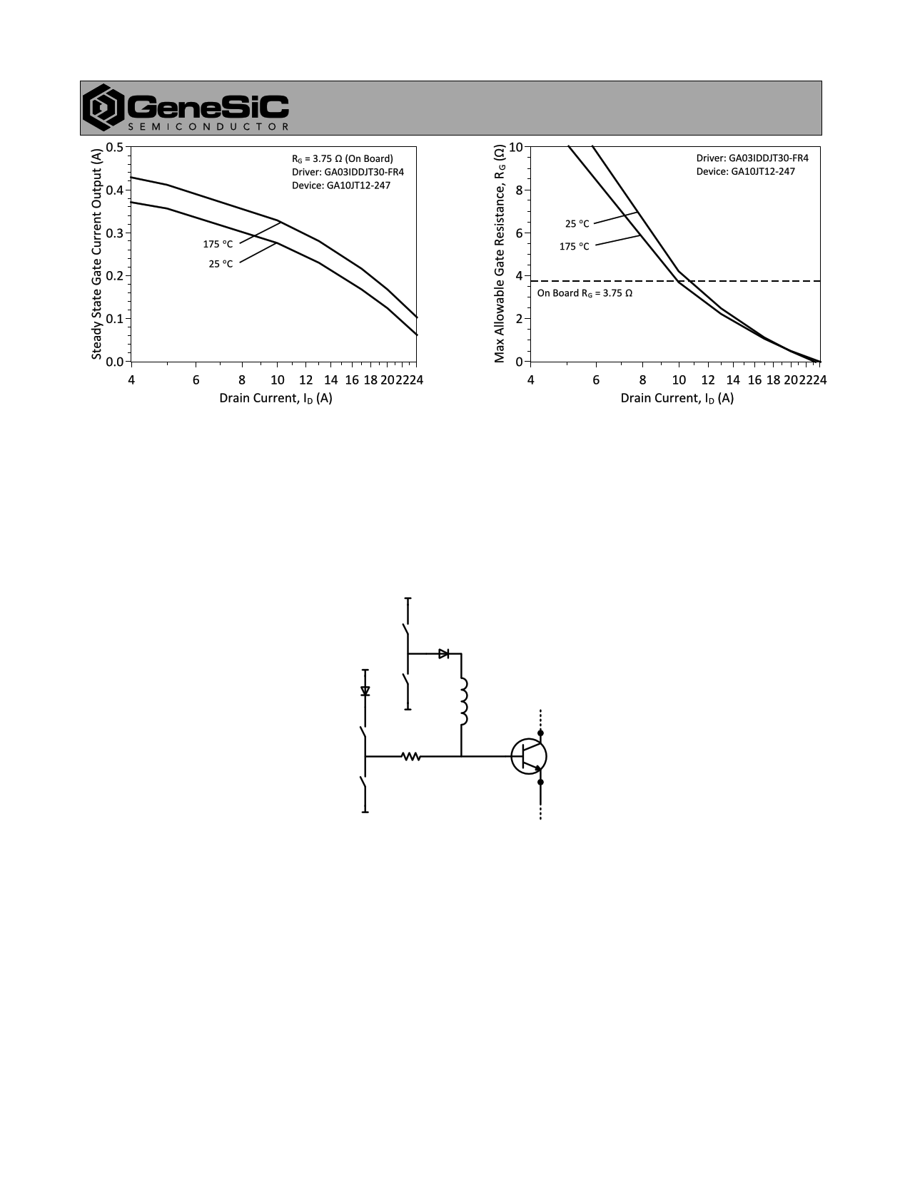
Figure 10: Typical steady state gate current supplied by the
GA03IDDJT30-FR4 board for the GA10JT06-CAL with the on
board resistance of 3.75 Ω
Figure 11: Maximum gate resistance for safe operation of
the GA10JT06-CAL at different drain currents using the
GA03IDDJT30-FR4 board.
B:2: High Speed, Low Loss Drive with Boost Inductor
A High Speed, Low-Loss Driver with Boost Inductor is also capable of driving the GA10JT06- CAL at high-speed. It utilizes a gate drive
inductor instead of a capacitor to provide the high-current gate current pulses IG,on and IG,off. During operation, inductor L is charged to a
specified IG,on current value then made to discharge IL into the SJT gate pin using logic control of S1, S2, S3, and S4, as shown in Figure 12.
After turn on, while the device remains on the necessary steady state gate current IG,steady is supplied from source VCC through RG. Please
refer to the article “A current-source concept for fast and efficient driving of silicon carbide transistors” by Dr. Jacek Rąbkowski for additional
information on this driving topology.4
VCC
S1
VCC
S2
VEE
S3
L
RG
S4
SiC SJT D
G
S
VEE
Figure 12: Simplified Inductive Pulsed Drive Topology
3 – RG = (1/RG1 +1/RG2)-1. Driver is pre-installed with RG1 = RG2 = 7.5 Ω
4 – Archives of Electrical Engineering. Volume 62, Issue 2, Pages 333–343, ISSN (Print) 0004-0746, DOI: 10.2478/aee-2013-0026, June 2013
Feb 2015
http://www.genesicsemi.com/high-temperature-sic/high-temperature-sic-bare-die/
Pg5 of 8
5 Page | ||
| Páginas | Total 9 Páginas | |
| PDF Descargar | [ Datasheet GA10JT06-CAL.PDF ] | |
Hoja de datos destacado
| Número de pieza | Descripción | Fabricantes |
| GA10JT06-CAL | OFF Silicon Carbide Junction Transistor | GeneSiC |
| Número de pieza | Descripción | Fabricantes |
| SLA6805M | High Voltage 3 phase Motor Driver IC. |
Sanken |
| SDC1742 | 12- and 14-Bit Hybrid Synchro / Resolver-to-Digital Converters. |
Analog Devices |
|
DataSheet.es es una pagina web que funciona como un repositorio de manuales o hoja de datos de muchos de los productos más populares, |
| DataSheet.es | 2020 | Privacy Policy | Contacto | Buscar |
