|
|
|
PDF HMC7992 Data sheet ( Hoja de datos )
| Número de pieza | HMC7992 | |
| Descripción | Nonreflective / Silicon SP4T Switch | |
| Fabricantes | Analog Devices | |
| Logotipo | ||
Hay una vista previa y un enlace de descarga de HMC7992 (archivo pdf) en la parte inferior de esta página. Total 13 Páginas | ||
|
No Preview Available !
Data Sheet
Nonreflective, Silicon SP4T Switch,
0.1 GHz to 6.0 GHz
HMC7992
FEATURES
Nonreflective, 50 Ω design
High isolation: 45 dB typical at 2 GHz
Low insertion loss: 0.6 dB at 2 GHz
High power handling
33 dBm through path
27 dBm terminated path
High linearity
1 dB compression (P1dB): 35 dBm typical
Input third-order intercept (IIP3): 58 dBm typical
ESD rating: 2 kV human body model (HBM), Class 2
Single positive supply: 3.3 V to 5.0 V
Standard TTL-, CMOS-, and 1.8 V-compatible control
16-lead, 3 mm × 3 mm LFCSP package (9 mm2)
Pin compatible with the HMC241ALP3E
APPLICATIONS
Cellular/4G infrastructure
Wireless infrastructure
Automotive telematics
Mobile radios
Test equipment
GENERAL DESCRIPTION
The HMC7992 is a general-purpose, nonreflective, 0.1 GHz to
6.0 GHz, silicon, single-pole, four-throw (SP4T) switch in a
leadless, surface-mount package. The switch is ideal for cellular
infrastructure applications, offers high isolation of 45 dB typical
at 2 GHz, and a low insertion loss of 0.6 dB at 2 GHz. It offers
excellent power handling capability up to 6.0 GHz, with input
power of 1 dB compression point (P1dB) of 35 dBm at 5 V
operation. The HMC7992 has good low frequency input power
handling below 0.1 GHz and can operate well down to 10 kHz,
with a typical 1 dB compression of 21 dBm (see Figure 21) and
an IIP3 of 37 dBm (see Figure 22) at 1 MHz.
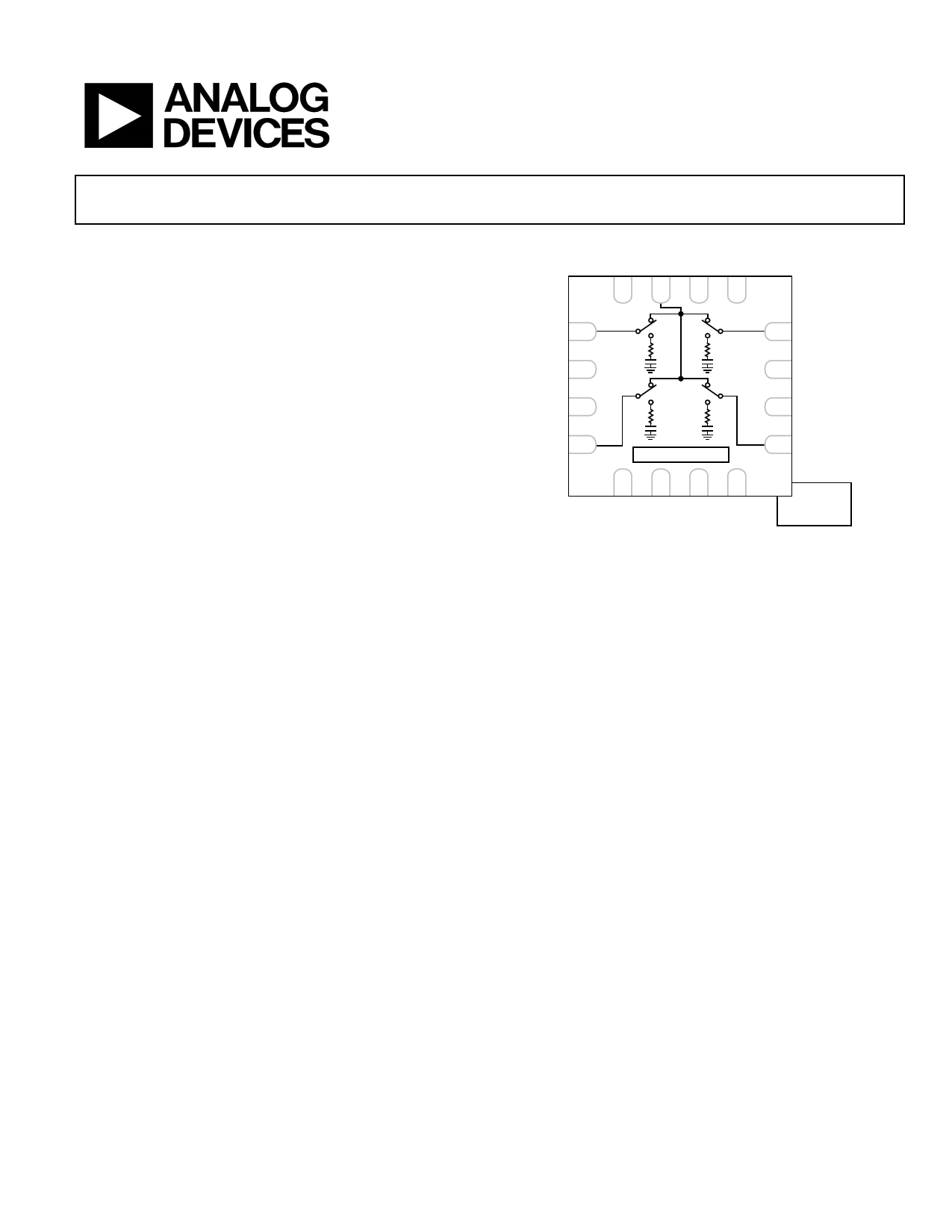
FUNCTIONAL BLOCK DIAGRAM
GND RFC GND GND
16 15 14 13
HMC7992
RF4 1
12 RF1
GND 2
11 GND
GND 3
10 GND
RF3 4
2:4 TTL DECODER
5
GND
6
VDD
7
B
8
A
Figure 1.
9 RF2
PACKAGE
BASE
GND
The on-chip circuitry allows the HMC7992 to operate at a single,
positive supply voltage range from 3.3 V to 5 V, and as well as a
single, positive control voltage from 0 V to 1.8 V/3.3 V/5.0 V. A
2:4 decoder integrated in the switch requires only two controlled
input signals, with a positive control voltage range from 0 V to
1.8 V/3.3 V/5.0 V, to select one of the four radio frequency (RF)
paths.
Rev. 0
Document Feedback
Information furnished by Analog Devices is believed to be accurate and reliable. However, no
responsibility is assumed by Analog Devices for its use, nor for any infringements of patents or other
rights of third parties that may result from its use. Specifications subject to change without notice. No
license is granted by implication or otherwise under any patent or patent rights of Analog Devices.
Trademarksandregisteredtrademarksarethepropertyoftheirrespectiveowners.
One Technology Way, P.O. Box 9106, Norwood, MA 02062-9106, U.S.A.
Tel: 781.329.4700
©2016 Analog Devices, Inc. All rights reserved.
Technical Support
www.analog.com
1 page 
Data Sheet
ABSOLUTE MAXIMUM RATINGS
Table 4.
Parameter
Bias Voltage Range (VDD)
Control Voltage Range (A, B)
RF Input Power,1 3.3 V to 5 V (see
Figure 2 and Figure 3)
Through Path
Terminated Path
Hot Switching
Channel Temperature
Storage Temperature Range
Maximum Peak Reflow Temperature
(MSL3)
Thermal Resistance (Channel to
Package Bottom)
Through Path
Terminated Path
ESD Sensitivity
Human Body Model (HBM)
Charged Device Model (CDM)
Rating
−0.3 V to +5.5 V
−0.5 V to VDD + (+0.5 V)
34 dBm
28 dBm
30 dBm
135°C
−65°C to +150°C
260°C
115°C
200°C
2 kV (Class 2)
1.25 kV
1 For recommended operating conditions, see Table 1.
Stresses at or above those listed under Absolute Maximum
Ratings may cause permanent damage to the product. This is a
stress rating only; functional operation of the product at these
or any other conditions above those indicated in the operational
section of this specification is not implied. Operation beyond
the maximum operating conditions for extended periods may
affect product reliability.
HMC7992
36
THROUGH AMR
34
32
30
28
TERMINATED AMR
26
24
0.1
1
FREQUENCY (GHz)
Figure 2. Maximum RF Input Power vs. Frequency
35
THROUGH (AT 85°C)
33
THROUGH (AT 105°C)
31
10
29
27
25 TERMINATED (AT 85°C)
23
TERMINATED (AT 105°C)
21
19
0.1
1
FREQUENCY (GHz)
Figure 3. Power Derating vs. Frequency
10
ESD CAUTION
Rev. 0 | Page 5 of 13
5 Page 
Data Sheet
THEORY OF OPERATION
The HMC7992 requires a single positive supply voltage applied
to the VDD pin. A bypassing capacitor is recommended on the
supply line to minimize RF coupling.
The HMC7992 integrates with an internal 2:4 decoder; the four
RF paths are selected via the two digital control voltages applied
to the A and B control inputs. A small value bypassing capacitor
is recommended on these digital signal lines to improve the RF
signal isolation.
The HMC7992 is internally matched to 50 Ω at the RF common
port (RFC) and the RF ports (RF1, RF2, RF3, and RF4); therefore,
no external matching components are required. The RF pins are
dc-coupled and dc blocking capacitors are required on the RF
paths. The design is bidirectional; the RF input signals can apply
at the RFC port or the RF1 to RF4 ports. The inputs and outputs
are interchangeable.
HMC7992
Depending on the logic level applied to the control input pins,
A and B, one RF output port (for example, RF1) is set to on
mode, by which an insertion loss path is provided from the
input to the output. The other RF output ports (for example,
RF2, RF3, and RF4) are then set to off mode, by which the
outputs are isolated from the input. When the RF output ports
(RF1, RF2, RF3, and RF4) are in isolation mode, they are
internally terminated to 50 Ω, and thereby can absorb the
applied RF signal.
The ideal power-up sequence is as follows:
1. Power up GND.
2. Power up VDD.
3. Power up the digital control inputs. The relative order of
the logic control inputs is not important. Powering the
logic control inputs before the VDD supply can inadvertently
forward bias and damage the internal ESD protection
structures.
4. Apply the RF input.
Table 7. Switch Mode Operation
Digital Control Inputs Signal Mode
AB
RFC to RFx
Low Low
RF Port 1 is in on mode, providing a low insertion loss path from the RFC port to the RF1 port. The remaining RF
ports (RF2, RF3, and RF4) are in off mode; they are isolated from the RFC port and internally terminated to a 50 Ω load.
High Low
RF Port 2 is in on mode, providing a low insertion loss path from the RFC port to the RF2 port. The remaining RF
ports (RF1, RF3, and RF4) are in off mode; they are isolated from the RFC port and internally terminated to a 50 Ω load.
Low High
RF Port 3 is in on mode, providing a low insertion loss path from the RFC port to the RF3 port. The remaining RF
ports (RF1, RF2, and RF4) are in off mode; they are isolated from the RFC port and internally terminated to a 50 Ω load.
High High
RF Port 4 is in on mode, providing a low insertion loss path from the RFC port to the RF4 port. The remaining RF
ports (RF1, RF2, and RF3) are in off mode; they are isolated from the RFC port and internally terminated to a 50 Ω load.
Rev. 0 | Page 11 of 13
11 Page | ||
| Páginas | Total 13 Páginas | |
| PDF Descargar | [ Datasheet HMC7992.PDF ] | |
Hoja de datos destacado
| Número de pieza | Descripción | Fabricantes |
| HMC7992 | Nonreflective / Silicon SP4T Switch | Analog Devices |
| HMC799LP3E | TRANSIMPEDANCE AMPLIFIER | Analog Devices |
| HMC799LP3E | 10 kOhm TRANSIMPEDANCE AMPLIFIER | Hittite Microwave Corporation |
| Número de pieza | Descripción | Fabricantes |
| SLA6805M | High Voltage 3 phase Motor Driver IC. |
Sanken |
| SDC1742 | 12- and 14-Bit Hybrid Synchro / Resolver-to-Digital Converters. |
Analog Devices |
|
DataSheet.es es una pagina web que funciona como un repositorio de manuales o hoja de datos de muchos de los productos más populares, |
| DataSheet.es | 2020 | Privacy Policy | Contacto | Buscar |