|
|
|
PDF XC9257 Data sheet ( Hoja de datos )
| Número de pieza | XC9257 | |
| Descripción | 1.0A Synchronous Step-Down DC/DC Converters | |
| Fabricantes | Torex Semiconductor | |
| Logotipo | ||
Hay una vista previa y un enlace de descarga de XC9257 (archivo pdf) en la parte inferior de esta página. Total 27 Páginas | ||
|
No Preview Available !
XC9257/XC9258 Series
COT Control, 1.0A Synchronous Step-Down DC/DC Converters
ETR05040-001
GENERAL DESCRIPTION
GreenOperation-compatible
The XC9257/XC9258 series is a group of synchronous-rectification type DC/DC converters with a built-in P-channel MOS driver
transistor and N-channel MOS switching transistor, designed to allow the use of ceramic capacitors. Output voltage is internally
set in a range from 0.8V to 3.6V (accuracy: ±2.0%) increments of 0.05V. The device provides a high efficiency, stable power
supply with an output current of 1.0A to be configured using only a coil and two capacitors connected externally. Oscillation
frequency is set to 1.2MHz or 6.0MHz can be selected for suiting to your particular application.
As for operation mode HiSAT-COT (*) control excellent in transient response, the XC9257 series is PWM control, the XC9258
series is automatic PWM/PFM switching control, allowing fast response, low ripple and high efficiency over the full range of loads
(from light load to heavy load).
During stand-by, all circuits are shutdown to reduce current consumption to as low as 1.0μA or less. As for the soft-start function
as fast as 0.3ms in typical for quick turn-on. With the built-in UVLO (Under Voltage Lock Out) function, the internal P-channel MOS
driver transistor is forced OFF when input voltage becomes 2.00V or lower. The B types integrate CL High Speed discharge
function which enables the electric charge at the output capacitor CL to be discharged via the internal discharge.
Two types of package SOT-25, USP-6C are available.
(*) HiSAT-COT is an original Torex term for High Speed Transient Response.
APPLICATIONS
FEATURES
Smart phones / Mobile phones
Input Voltage Range
Output Voltage Range
: 2.5V 5.5V
: 0.8V 3.6V (±2.0%)
Bluetooth
Oscillation Frequency
: 1.2MHz, 6.0MHz
Portable game consoles
Digital still cameras / Camcorders
Output Current
Control Methods
: 1A
: HiSAT-COT Control
100% Duty Cycle
Point-of-Load (POL)
Wearable devices
Protection Circuits
PWM Control (XC9257)
PWM/PFM Auto (XC9258)
: Thermal Shutdown
Current Limit (Pendent character)
Short Circuit Protection (Type B)
Functions
: Soft-Start
UVLO
CL High Speed Discharge (Type B)
Capacitor
: Ceramic Capacitor
Operating Ambient Temperature : - 40
+ 105
Packages
: SOT-25, USP-6C
Environmentally Friendly
: EU RoHS Compliant, Pb Free
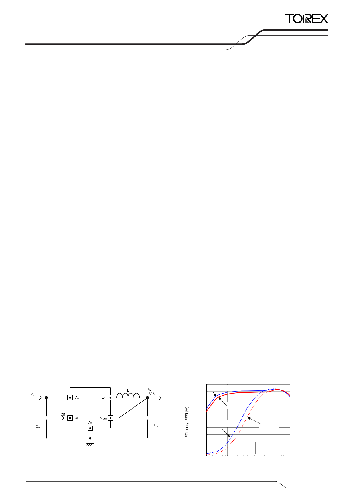
TYPICAL APPLICATION CIRCUIT
TYPICAL PERFORMANCE
CHARACTERISTICS
XC9257B18C/XC9258B18C
L =LTF5022T-4R7N2R0(4.7 H)
CIN = 10 F(GRM155R61A106M) CL = 10
100
F(GRM155R61A106M
90
80
70
60
50
40
30
20
10
0
0.1
1 10 100
Output Current: IOUT (mA)
1000
1/27
1 page 
ABSOLUTE MAXIMUM RATINGS
PARAMETER
VIN Pin Voltage
SYMBOL
VIN
RATINGS
-0.3 +6.2
Ta=25
UNITS
V
Lx Pin Voltage
VLx
-0.3 VIN+0.3 or +6.2(*1)
V
VOUT Pin Voltage
VOUT
-0.3 VIN+0.3 or +4.0(*2)
CE Pin Voltage
Power Dissipation
SOT-25
USP-6C
VCE
Pd
-0.3 +6.2
250
600 (PCB mounted)
120
1000 (PCB mounted)
Operating Ambient Temperature Topr
-40 +105
Storage Temperature
Tstg
-55 +125
* All voltages are described based on the GND (VSS) pin.
(*1) The maximum value should be either VIN+0.3V or +6.2V in the lowest.
(*2) The maximum value should be either VIN+0.3V or +4.0V in the lowest.
V
V
mW
XC9257/XC9258
Series
5/27
5 Page 
XC9257/XC9258
Series
OPERATIONAL EXPLANATION
The XC9257/XC9258 series consists of a reference voltage source, error amplifier, comparator, phase compensation, minimum
on time generation circuit, output voltage adjustment resistors, P-channel MOS driver transistor, N-channel MOS switching
transistor for the synchronous switch, current limiter circuit, UVLO circuit, thermal shutdown circuit, short protection circuit,
PWM/PFM selection circuit and others. (See the BLOCK DIAGRAM below.)
BLOCK DIAGRAM XC9257/XC9258 Series Type B (SOT-25)
The method is HiSAT-COT (High Speed circuit Architecture for Transient with Constant On Time) control, which features on
time control method and a fast transient response that also achieves low output voltage ripple.
The on time (ton) is determined by the input voltage and output voltage, and turns on the Pch MOS driver Tr. for a fixed time.
During the off time (toff), the voltage that is fed back through R1 and R2 is compared to the reference voltage by the error amp,
and the error amp output is phase compensated and sent to the comparator. The comparator compares this signal to the
reference voltage, and if the signal is lower than the reference voltage, sets the SR latch. On time then resumes. By doing this,
PWM operation takes place with the off time controlled to the optimum duty ratio and the output voltage is stabilized. The phase
compensation circuit optimizes the frequency characteristics of the error amp, and generates a ramp wave similar to the ripple
voltage that occurs in the output to modulate the output signal of the error amp. This enables a stable feedback system to be
obtained even when a low ESR capacitor such as a ceramic capacitor is used, and a fast transient response and stabilization of
the output voltage are achieved.
<Minimum on time generation circuit>
Generates an on time that depends on the input voltage and output voltage (ton). The on time is set as given by the equations
below.
fOSC 1.2MHz type
ton (us) = VOUT/VIN 0.833
fOSC 6.0MHz type
ton (us) = VOUT/VIN 0.167
<Switching frequency>
The switching frequency can be obtained from the on time (ton), which is determined by the input voltage and output voltage,
and the PWM controlled off time (toff) as given by the equation below.
fOSC (MHz) = VOUT(V) / (VIN(V) ton(us))
<100% duty cycle mode>
When the load current is heavy and the voltage difference between input voltage and output voltage is small, 100% duty cycle
mode is activated and it keeps the Pch MOS driver Tr. keep on. 100% duty cycle mode attains a high output voltage stability and
a high-speed response under all load conditions, from light to heavy, even in conditions where the dropout voltage is low.
<Error amp>
The error amp monitors the output voltage. The voltage divided by the internal R1 and R2 resistors is a feedback voltage for
Error Amp. and compared to the reference voltage. The output voltage of the error amp becomes higher when the feedback
voltage is higher than the reference voltage. The frequency characteristics of the error amp are optimized internally.
11/27
11 Page | ||
| Páginas | Total 27 Páginas | |
| PDF Descargar | [ Datasheet XC9257.PDF ] | |
Hoja de datos destacado
| Número de pieza | Descripción | Fabricantes |
| XC9250 | 30V Driver Transistor Built-In Step-Down DC/DC Converters | Torex Semiconductor |
| XC9251 | 30V Driver Transistor Built-In Step-Down DC/DC Converters | Torex Semiconductor |
| XC9252 | Low Power Consumption Step-down DC/DC Controller IC | Torex Semiconductor |
| XC9253R | Synchronous Step-Down DC/DC Converter | Torex Semiconductor |
| Número de pieza | Descripción | Fabricantes |
| SLA6805M | High Voltage 3 phase Motor Driver IC. |
Sanken |
| SDC1742 | 12- and 14-Bit Hybrid Synchro / Resolver-to-Digital Converters. |
Analog Devices |
|
DataSheet.es es una pagina web que funciona como un repositorio de manuales o hoja de datos de muchos de los productos más populares, |
| DataSheet.es | 2020 | Privacy Policy | Contacto | Buscar |