|
|
|
PDF LM2460 Data sheet ( Hoja de datos )
| Número de pieza | LM2460 | |
| Descripción | Monolithic Triple Channel High Swing CRT Driver | |
| Fabricantes | National Semiconductor | |
| Logotipo | ||
Hay una vista previa y un enlace de descarga de LM2460 (archivo pdf) en la parte inferior de esta página. Total 11 Páginas | ||
|
No Preview Available !
September 2003
LM2460
Monolithic Triple Channel High Swing CRT Driver
General Description
The LM2460 is an integrated high voltage CRT driver circuit
designed for use in high brightness monitor applications. The
IC contains three high input impedance, wide band amplifi-
ers which directly drive the RGB cathodes of a CRT. Each
channel has its gain internally set to −30 and can drive CRT
capacitive loads as well as resistive loads present in other
application, limited only by the package’s power dissipation.
The IC is packaged in an industry standard 9 lead TO-220
molded plastic package.
n Stable with 0–20 pF capacitive loads and inductive
peaking networks
n Convenient TO-220 staggered lead package style
n Matched to LM126X/3X/4X pre-amplifier families
Applications
n High brightness CRT monitors
Features
n 0V to 5V input range
n Capable of up to a 70 Vp-p output swing
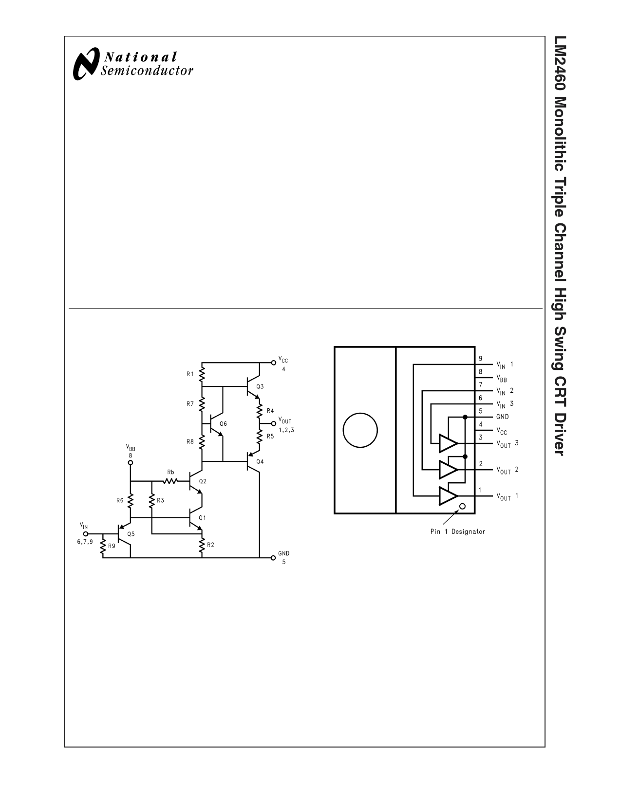
Schematic and Connection Diagrams
20082601
FIGURE 1. Simplified Schematic Diagram (One
Channel)
Top View
20082602
Order Number LM2460TA
See NS Package Number TA09A
© 2003 National Semiconductor Corporation DS200826
www.national.com
1 page 
Theory of Operation
The LM2460 is a high voltage monolithic three channel CRT
driver with a higher output swing suitable for driving the new
high brightness CRTs. The LM2460 operates with 120V and
8V power supplies. The part is housed in the industry stan-
dard 9-lead TO-220 molded plastic power package.
The circuit diagram of the LM2460 is shown in Figure 1. The
PNP emitter follower, Q5, provides input buffering. Q1 and
Q2 form a fixed gain cascode amplifier with resistors R1 and
R2 setting the gain at −32. Emitter followers Q3 and Q4
isolate the high output impedance of the amplifier from the
capacitive load on the output of the amplifier, decreasing the
sensitivity of the device to changes in load capacitance. Q6
provides biasing to the output emitter follower stage to re-
duce crossover distortion at low signal levels.
Figure 2 shows a typical test circuit for evaluation of the
LM2460. This circuit is designed to allow testing of the
LM2460 in a 50Ω environment without the use of an expen-
sive FET probe. In this test circuit, two low inductance resis-
tors in series totaling 4.95 kΩ form a 200:1 wideband, low
capacitance probe when connected to a 50Ω coaxial cable
and a 50Ω load (such as a 50Ω oscilloscope input). The
input signal from the generator is AC coupled to the base of
Q5. VBIAS is used to adjust the DC level of the output.
Application Hints
INTRODUCTION
National Semiconductor (NSC) is committed to provide ap-
plication information that assists our customers in obtaining
the best performance possible from our products. The fol-
lowing information is provided in order to support this com-
mitment. The reader should be aware that the optimization of
performance was done using a specific printed circuit board
designed at NSC. Variations in performance can be realized
due to physical changes in the printed circuit board and the
application. Therefore, the designer should know that com-
ponent value changes may be required in order to optimize
performance in a given application. The values shown in this
document can be used as a starting point for evaluation
purposes. When working with high bandwidth circuits, good
layout practices are also critical to achieving maximum per-
formance.
IMPORTANT INFORMATION
The LM2460 performance is targeted for the 15" and 17"
market with resolutions up to 1024 x 7684 and 75 Hz refresh
rate. It is designed to be a replacement for discrete CRT
drivers. The application circuits shown in this document to
optimize performance and to protect against damage from
CRT arc-over are designed specifically for the LM2460. If
another member of the LM246X family is used, please refer
to its datasheet.
POWER SUPPLY BYPASS
Since the LM2460 is a wide bandwidth amplifier, proper
power supply bypassing is critical for optimum performance.
Improper power supply bypassing can result in large over-
shoot, ringing or oscillation. A 0.1 µF capacitor should be
connected from the supply pin, VCC, to ground, as close to
the supply and ground pins as is practical. Additionally, a
22 µF to 100 µF electrolytic capacitor should be connected
from the supply pin to ground. The electrolytic capacitor
should also be placed reasonably close to the LM2460’s
supply and ground pins. A 0.1 µF capacitor should be con-
nected from the bias pin (VBB) to ground, as close as is
practical to the part.
ARC PROTECTION
During normal CRT operation, internal arcing may occasion-
ally occur. Spark gaps, in the range of 200V, connected from
the CRT cathodes to CRT ground will limit the maximum
voltage, but to a value that is much higher than allowable on
the LM2460. This fast, high voltage, high energy pulse can
damage the LM2460 output stage. The application circuit
shown in Figure 9 is designed to help clamp the voltage at
the output of the LM2460 to a safe level. The clamp diodes,
D1 and D2, should have a fast transient response, high peak
current rating, low series impedance and low shunt capaci-
tance. FDH400 or equivalent diodes are recommended. Do
not use 1N4148 diodes for the clamp diodes. D1 and D2
should have short, low impedance connections to VCC and
ground respectively. The cathode of D1 should be located
very close to a separately decoupled bypass capacitor (C3 in
Figure 9). The ground connection of D2 and the decoupling
capacitor should be very close to the LM2460 ground. This
will significantly reduce the high frequency voltage transients
that the LM2460 would be subjected to during an arcover
condition. Resistor R2 limits the arcover current that is seen
by the diodes while R1 limits the current into the LM2460 as
well as the voltage stress at the outputs of the device. R2
should be a 1/2W solid carbon type resistor. R1 can be a
1/4W metal or carbon film type resistor. Having large value
resistors for R1 and R2 would be desirable, but this has the
effect of increasing rise and fall times. Inductor L1 is critical
to reduce the initial high frequency voltage levels that the
LM2460 would be subjected to. The inductor will not only
help protect the device but it will also help optimize rise and
fall times as well as minimize EMI. For proper arc protection,
it is important to not omit any of the arc protection compo-
nents shown in Figure 9.
20082609
FIGURE 9. One Channel of the LM2460 with the
Recommended Application Circuit
OPTIMIZING TRANSIENT RESPONSE
Referring to Figure 9, there are three components, (R1, R2
and L1) that can be adjusted to optimize the transient re-
sponse of the application circuit. Increasing the values of R1
and R2 will slow the circuit down while decreasing over-
shoot. Increasing the value of L1 will speed up the circuit as
well as increase overshoot. It is very important to use induc-
tors with very high self-resonant frequencies, perferably
above 300 MHz. Ferrite core inductors from J.W. Miller
Magnetics (part # 78FR--K) were used for optimizing the
performance of the device in the NSC application board. The
values shown in Figure 9 can be used as a good starting
point for the evaluation of the LM2460. Using a variable
5 www.national.com
5 Page 
Physical Dimensions inches (millimeters) unless otherwise noted
NS Package Number TA09A
Order Number LM2460TA
LIFE SUPPORT POLICY
NATIONAL’S PRODUCTS ARE NOT AUTHORIZED FOR USE AS CRITICAL COMPONENTS IN LIFE SUPPORT
DEVICES OR SYSTEMS WITHOUT THE EXPRESS WRITTEN APPROVAL OF THE PRESIDENT AND GENERAL
COUNSEL OF NATIONAL SEMICONDUCTOR CORPORATION. As used herein:
1. Life support devices or systems are devices or
systems which, (a) are intended for surgical implant
into the body, or (b) support or sustain life, and
whose failure to perform when properly used in
accordance with instructions for use provided in the
labeling, can be reasonably expected to result in a
significant injury to the user.
2. A critical component is any component of a life
support device or system whose failure to perform
can be reasonably expected to cause the failure of
the life support device or system, or to affect its
safety or effectiveness.
National Semiconductor
Americas Customer
Support Center
Email: [email protected]
Tel: 1-800-272-9959
www.national.com
National Semiconductor
Europe Customer Support Center
Fax: +49 (0) 180-530 85 86
Email: [email protected]
Deutsch Tel: +49 (0) 69 9508 6208
English Tel: +44 (0) 870 24 0 2171
Français Tel: +33 (0) 1 41 91 8790
National Semiconductor
Asia Pacific Customer
Support Center
Email: [email protected]
National Semiconductor
Japan Customer Support Center
Fax: 81-3-5639-7507
Email: [email protected]
Tel: 81-3-5639-7560
National does not assume any responsibility for use of any circuitry described, no circuit patent licenses are implied and National reserves the right at any time without notice to change said circuitry and specifications.
11 Page | ||
| Páginas | Total 11 Páginas | |
| PDF Descargar | [ Datasheet LM2460.PDF ] | |
Hoja de datos destacado
| Número de pieza | Descripción | Fabricantes |
| LM246 | PROGRAMMABLE QUAD BIPOLAR OPERATIONAL AMPLIFIERS | STMicroelectronics |
| LM2460 | LM2460 Monolithic Triple Channel High Swing CRT Driver (Rev. B) | Texas Instruments |
| LM2460 | Monolithic Triple Channel High Swing CRT Driver | National Semiconductor |
| LM2462 | LM2462 Monolithic Triple 3 ns CRT Driver | Texas Instruments |
| Número de pieza | Descripción | Fabricantes |
| SLA6805M | High Voltage 3 phase Motor Driver IC. |
Sanken |
| SDC1742 | 12- and 14-Bit Hybrid Synchro / Resolver-to-Digital Converters. |
Analog Devices |
|
DataSheet.es es una pagina web que funciona como un repositorio de manuales o hoja de datos de muchos de los productos más populares, |
| DataSheet.es | 2020 | Privacy Policy | Contacto | Buscar |